Gallium Arsenide (GaAs) Wafer is a critical sort III-V direct bandgap semiconductor utilized in different gadgets like infrared discharging diodes, laser diodes, and microwave recurrence coordinated circuits. It is likewise used in the development of photovoltaic cells.
Then again, Gallium Arsenide Wafers, the monetarily accessible type of GaAs, hold a vital job in the semiconductor business. They fundamentally act as stages or substrates in an epitaxial design for the development of extra semiconductor materials. Their specialized purposes incorporate the combination of type III-V semiconductors and superior execution optoelectronic gadgets like high-thickness p-I-n finders and laser diodes with strong silicon electronic coordinated circuits. This mix is done solidly to make sturdy circuits with a scope of uses. Quanto Nano’s Gallium Arsenide (GaAs) wafer items give great sign transmission in high-recurrence applications, on account of their elite exhibition and wide bandwidth.
Introduction
Gallium arsenide (GaAs) is a compound of gallium and arsenic. It is an imperative semiconductor and is usually used to produce gadgets like infrared transmitting diodes, laser diodes, incorporated circuits at microwave frequencies, and photovoltaic cells.
Gallium arsenide (GaAs) wafers are pivotal parts in the assembling of different electronic gadgets. These wafers comprise of single precious stones of gallium arsenide, having remarkable electrical and optical properties. GaAs wafers are regularly developed utilizing procedures like sub-atomic pillar epitaxy (MBE) or metalorganic fume stage epitaxy (MOVPE). GaAs is an III-V compound semiconductor with a direct bandgap, considering effective emanation and retention of light in the infrared and noticeable light range. GaAs wafers have high electron portability, outperforming that of silicon, making them reasonable for rapid applications like microwave gadgets, fast semiconductors, and coordinated circuits (ICs).
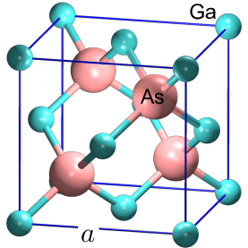
Structure of Gallium Arsenide (GaAs) Wafer
In the Gallium arsenide (GaAs) wafer, every gallium molecule is lined by arsenic particles. 5 valence electrons of arsenic molecules and 3 valence electrons of gallium iotas share one another. Thus, every one of the gallium and arsenic iota gets 8 valence electrons in the external shell. It is likewise to be noticed that a covalent bond exists among gallium and arsenic particle in the GaAs Wafer. The covalent bonds in spite of areas of strength for being be broken with an enough measure of outside energy.
Preparation Strategies for Gallium Arsenide Wafers
Fume stage Epitaxial (VPE) development strategy: VPE is a technique to store a few layers of material onto a substrate. In this strategy, an unstable forerunner goes through a substance change at a surface, bringing about a strong store. The response can be improved by the expansion of gases like hydrogen or argon. This procedure can deliver exceptionally uniform movies with great material properties.
Gradient Freeze (GF) method: This strategy is frequently utilized for making single-gem materials. As you depicted, the cycle includes cautiously controlling the temperature in the heater to step by step cement a dissolve, which considers the development of a solitary gem. The advantage of this technique is that the gem that is created is regularly excellent and has a low imperfection thickness.
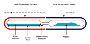
Liquid-stage Epitaxial (LPE) development method: LPE is a strategy used to develop single-gem semiconductor layers from a dissolve on a substrate. It’s frequently utilized for assembling parts of electronic and optoelectronic gadgets, like LEDs.
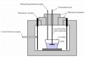
Liquid-typified Czochralski (LEC) method: This strategy is utilized to develop single precious stones of materials, especially semiconductors like gallium arsenide. The gem is drawn from a dissolve which is held inside a reasonable cauldron and is shielded from defilement by being embodied by a fluid, consequently the name.
**
Atomic Shaft Epitaxy (MBE) and Metal-Natural Compound Fume Testimony (MO-CVD)**: These are fresher strategies for making gallium arsenide wafers. MBE includes the collaboration of a light emission or more thermalized natural or compound sources with a warmed surface. Metal-natural synthetic fume testimony is a flexible procedure for developing slender movies of different materials. Both of these procedures consider the development of profoundly controlled, top notch layers of material.
Bridgman-Stockbarger technique: This is one more strategy for developing single-gem materials. The essential reason includes moving the material to be cemented gradually through a temperature inclination. At the hot end, the material is liquid, and at the virus end, it’s strong.
Properties of Gallium Arsenide (GaAs) Wafer
The principal properties of gallium arsenide (GaAs) are given underneath:
- The Molar mass of Gallium
arsenide (GaAs) is 144.64 g/mol. - Gallium arsenide (GaAs) has the
Liquefying point of 1238 °C. - The thickness of Gallium arsenide
(GaAs) is 5.32 g/cm3.
Gallium has better electronic properties looked at than silicon, like higher electron portability and immersed electron speed. This permits gallium arsenide to work at frequencies up to 250 GHz in semiconductors. It is less delicate to high temperatures, produces less clamor in electronic circuits, and gives effective light retention and discharge because of its immediate bandgap. Gallium arsenide’s resistive nature and high dielectric steady make it an optimal substrate for coordinated circuits, offering regular confinement between parts. These properties make gallium arsenide a promising possibility for applications in satellites, cell phones, correspondence innovation, and solid microwave coordinated circuits (MMICs). Wafers, which are dainty semiconductor layers utilized in microelectronic gadgets, go through alterations like particle implantation, doping, meager film statement, and drawing to be applied actually.
Use of Gallium Arsenide (GaAs) Wafer
The primary utilization of gallium arsenide (GaAs) is seen as in:
- Computers
- Photovoltaic cells
- Optoelectronic communications
- Laser diodes and infrared emission
GaAs Wafers’ Utilization in Semiconductors & Computers
Gallium arsenide wafer, a parallel compound framed from the component gallium and arsenic, presents fabricating difficulties in the creation of semiconductors because of its lower warm conductivity and higher coefficient of warm extension (CTE) contrasted with rudimentary semiconductors like silicon and germanium. Also, understanding gadget disappointments in view of GaAs can be more perplexing and exorbitant than those in light of silicon because of its somewhat ongoing reception. In any case, while thinking about the equilibrium of value, cost, and the additional worth of GaAs, these confusions are offset. The developing business sectors, requesting innovation that empowers higher frequencies, add to the offset of these expenses.
GaAs Wafers’ Utilization in Guard & Aerospace
Gallium arsenide has been integrated into business marketssince its utilization started for the military and aviation field. It has a place with the semiconductor materials bunch in the occasional table. The width of the band hole is more noteworthy than in silicon or germanium. The portability of the electrons is additionally more noteworthy than in silicon or germanium, and that of the openings like those of silicon.
To impurify the sort p, materials, for example, zinc, cadmium or copper are utilized since they present allowed levels in the scope of 0.08 to 0.37 eV over the valence band of GaAs. The giver materials are sulfur, selenium and the components of gathering IV of the occasional table, in little fixation, assuming they supplant gallium particles.
The GaAs is utilized for photoelectric cells, burrowing diodes, lasers, semiconductors and MESFET semiconductors.
The GaAs has a few circuit geographies and gadget types. The most predominant and industrially accessible is the FET rationale straightforwardly combined with DCFL (Direct Coupled FET Rationale), in spite of the fact that BFL rationale (Cradled FET Rationale) and SDFL rationale (Schottky Diode FET Rationale) are likewise accessible
GaAs Wafers Use in High recurrence Technologies
The powerful mass of the electric charge of the doped N-type GaAs is lower than in the silicon of a similar kind, so the electrons in GaAs Wafers are advanced at higher velocities, getting some margin to cross the semiconductor channel. This is extremely helpful at high frequencies, since a higher greatest working recurrence will be reached.
This chance and need to work with circuits that permit to act at higher frequencies has its starting point in the guard and space enterprises, in the utilization of radars, secure correspondences and sensors. After advancement by government programs, GaAs before long extended to new ad showcases, for example, remote neighborhood (WLAN), individual correspondence frameworks (laptops), live satellite transmission (DBS), transmission and gathering by the shopper, worldwide situating frameworks (GPS) and versatile interchanges. This multitude of business sectors required working at high and low frequencies that couldn’t be accomplished with silicon or germanium.

Advantages of Gallium Arsenide (GaAs) Wafers
The benefit of gallium arsenide wafers over sun powered grade silicon wafers is that it offers two times the productivity. One more benefit of GaAs wafer alludes to the expansion in effectiveness. Generally the gallium arsenide is kept in a solitary slim layer on a little sheet, yet at the College of Illinois, various layers of material have been saved on the wafers, getting a better return. Different layers dispense with the restrictions in the space of work, something vital on account of sunlight based cells, which require a wide inclusion region to catch however much light as could reasonably be expected. In this manner, a more noteworthy area of inclusion is accomplished, creating more energy and lower cost. The utilization of arsenide in sun oriented cells isn’t new. It has been utilized for a long time in the multi-intersection cells.
Disadvantages of Gallium Arsenide (GaAs) Wafers
The gadgets made with GaAs wafers can work at temperatures of up to 450 °C. In any case, in spite of this benefits, its utilization represents a few troubles, contrasted and that of silicon. For instance, not at all like silicon, there is no regular oxide that goes about as a veil to create basic components of the CMOS rationale style.
The huge detriment, which makes sense of its low usage, is the cost. To tackle this problem, designers and scientists say they have accomplished new strategies for assembling slim movies of minimal expense gallium arsenide, which would make gadgets that would supplant silicon, thus expanding the productivity of photovoltaic cells.
Conclusion
Gallium arsenide (GaAs) contains a molecule of Gallium and one more particle of Arsenide. Its utilization is ordinarily tracked down in hardware, like in the assembling of semiconductors. The compound enjoys a few benefits and impediments, as portrayed previously. The work is in progress to control the cost of this compound and there is significantly more that Gallium arsenide (GaAs) Wafers can propose in different areas too. In this way, the examination should be kept on finding its outstanding purposes. Visit Quanto Nano to upgrade your activities and research and find our state of the art items.