Contents
Introduction
Semiconductors represent one of the world’s most important industries, the core technology that powers the modern digital world.[1] Recognizing this vital role, China’s government has prioritized the sector, investing hundreds of billions of dollars to catalyze the development of an indigenous semiconductor ecosystem and to ideally cultivate globally competitive semiconductor firms across virtually all segments of the semiconductor value chain, from semiconductor design and fabrication to assembly, test, and packaging (ATP).
Thus far, those efforts have met with uneven success. With regard to the fabrication of leading-edge logic semiconductor chips, China’s flagship competitor, the Semiconductor Manufacturing International Corporation (SMIC), likely stands about five years behind global leaders such as the Taiwan Semiconductor Manufacturing Company (TSMC). Chinese companies As G. Dan Hutcheson, vice chair of research firm TechInsights, explained, “Ten years ago, [Chinese companies] were two generations behind. Five years ago, they were two generations behind, and now they’re still two generations behind.” Chinese firms Chinese competitors are even further behind with regard to semiconductor manufacturing equipment (SME), such as the lithography tools that make semiconductors: One commentator noted that Chinese firms might be as many as five generations behind in this field. The best machinery a Chinese company can produce makes chips that are 28 nanometers wide; the industry’s cutting-edge equipment can make 2-nanometer chips. As one analyst explained, “The best machinery a Chinese company can produce makes chips that are 28 nanometers wide; the industry’s cutting-edge equipment can make 2-nanometer chips.”
That said, Chinese semiconductor firms appear to be catching up in certain pockets: for instance, industry analysts view the design attributes and features of Huawei’s Mate 60 Pro smartphone as within 18 to 24 months of competitors’ versions. China has also made inroads in the production of legacy semiconductors (those greater than 28 nanometers), although Chinese firms appear to be competing in this sector on a more price- than innovation-intensive basis. In total, China continues to lag behind global leaders in most facets of semiconductor design and fabrication, but its firms’ intellectual property (IP) and innovation capabilities are accelerating rapidly as China pursues an aggressive whole-of-society strategy in an intense state-directed effort to achieve domestic semiconductor self-sufficiency.
A Brief Overview of the Global Semiconductor Industry
Modern semiconductors contain billions of transistors on a chip the size of a square centimeter, with circuits measured at the nanoscale (“nm,” a unit of length equal to one billionth of a meter). The very newest semiconductor fabrication facilities, which can cost over $30 billion to construct, produce semiconductors at 3 or 2nm (and even sub-2 nm) scales.6
The semiconductor sector is a $527 billion global industry that’s expected to become a trillion-dollar one by 2030.[7] Over 70 new semiconductor fabs are expected to be constructed worldwide by 2030 to satisfy this growing demand.[8] In short, semiconductors represent the commanding heights of the modern global digital economy, and this explains why leadership in the sector is so fiercely contested among nations, not least the People’s Republic of China (PRC), the European Union nations, Japan, South Korea, Taiwan, and the United States.
Computer circuit board technology (with processor), close up. Modern semiconductors contain billions of transistors on a chip the size of a square centimeter, with circuits measured at the nanoscale.
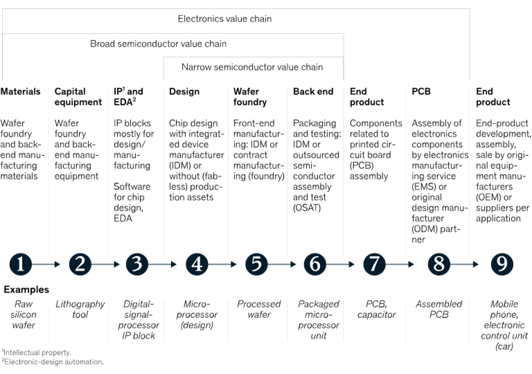
The semiconductor production process represents perhaps the most complex engineering task humanity undertakes. When all production phases are considered, the entire semiconductor production process extends from raw material procurement to end-product manufacturing.9 (See figure 1.) The core (or “narrow”) steps of the semiconductor production process include chip design, chip fabrication, and back-end ATP, with these steps supported by key inputs such as electronic design automation (EDA) software and SME such as lithography, deposition, and etch tooling.
Semiconductors represent one of the world’s most important industries, the core technology powering the modern digital world and empowering innovation and productivity growth across every industry.
Lithography, wherein a chip wafer gets inserted into a lithography machine and exposed to deep ultraviolet (DUV) or extreme ultraviolet (EUV) light and a pattern is printed onto a chip’s resist layer through a photomask, in particular represents a crucial step in the chipmaking process. EUV represents the latest and most sophisticated lithography technology, which Dutch firm ASML having invested €6 billion ($6.5 billion) to innovate over the past 17 years.10 The October 2022 export controls the United States placed on China included restrictions on equipment that can manufacture chips below 20 nm (impacting both DUV and EUV).11 In June 2023, the United States brokered a deal with the Netherlands to restrict exports of leading-edge EUV equipment to China.12
Figure 1: Facets of the semiconductor value chain[13]
The four most prevalent types of semiconductors are logic chips, memory chips (usually dynamic random-access memory (DRAM) or NAND “flash”), analog chips (those which generate a signal or transform signal characteristics, and are especially prevalent in automotive and audio applications), and power chips (those used as a switch in power electronics). “Advanced” or leading-edge logic chips are generally viewed as being sub-14 nm, while “legacy” (often called “mature-node”) chips refer to those manufactured using 28 nm or larger technology processes. Legacy chips are especially common in automobiles, medical devices, household appliances, energy, infrastructure, and aerospace products.
Lastly, several key business models define the industry. Integrated device manufacturers (IDMs) characterize firms—such as Infineon, Intel, Micron, Renesas, Samsung, SK Hynix, and Texas Instruments—which conduct all key facets of semiconductor manufacturing, especially design and fabrication, internally. Foundries such as Global Foundries, SMIC, and TSMC specialize solely in semiconductor manufacturing, often of the chip designs developed by “fabless” companies that specialize in designing application-specific chips, such as Advanced Micro Devices (AMD), chips for AI, high-performance computing (HPC), and graphics, Apple (mobile devices), NVIDIA (AI chips), or Qualcomm (5G and other wireless chips). [14]
Background and Methodology
The common narrative is that China is a copier and the United States is an innovator. That narrative often supports a lackadaisical attitude toward U.S. technology and industrial policy. After all, America leads (almost by right) in innovation, so there is nothing to worry about. But, first, this assumption is misguided because it is possible for innovators to lose leadership to copiers with lower cost structures, as has been the case in many U.S. industries, including consumer electronics, solar panels, telecom equipment, and machine tools.[15] Second, it’s not clear that China is a sluggish copier that’s always destined to be a follower.
To assess how innovative Chinese industries are, the Smith Richardson Foundation provided support to the Information Technology and Innovation Foundation (ITIF) to research this question. As part of this research, ITIF is reviewing particular sectors, including semiconductors.
To be sure, it is difficult to assess the innovation capabilities of any country’s industries, but it is especially difficult for Chinese industries. In part, this is because, under President Xi Jinping, China discloses much less information to the world than it used to, especially about its industrial and technological capabilities. Indeed, as The Economist wrote, “China’s chip industry operates under a shroud of secrecy. Breakthroughs and setbacks are often deemed to be state secrets, the divulgence of which can result in arrest.” [16]
Notwithstanding this, ITIF relied on three methods to assess Chinese innovation in semiconductors. First, we conducted in-depth case study evaluations of several Chinese semiconductor companies randomly selected from companies listed on the “2023 EU Industrial R&D Investment Scoreboard.” Second, we conducted interviews and held a focus group roundtable with global experts on the Chinese semiconductor industry. And, third, we assessed global data on semiconductor innovation, including scientific articles and patents. This report provides ITIF’s assessment of China’s current level of innovativeness in the semiconductor sector and offers a forward-looking perspective based upon rapidly evolving trendlines.
Importance of Semiconductors and the U.S. Role
The United States invented the semiconductor industry, harkening back to 1947, when Bell Labs’ John Bardeen, Walter Brattain, and William Shockley invented the transistor, a semiconductor device used to amplify or switch electronic signals and electrical power. In the mid-1950s, Jack Kilby at Texas Instruments and Robert Noyce and a team of researchers at Fairchild Semiconductor pioneered the integrated circuit (IC), placing multiple transistors on a single flat piece of semiconductor material, giving rise to the modern visage of a “semiconductor chip.”[17]
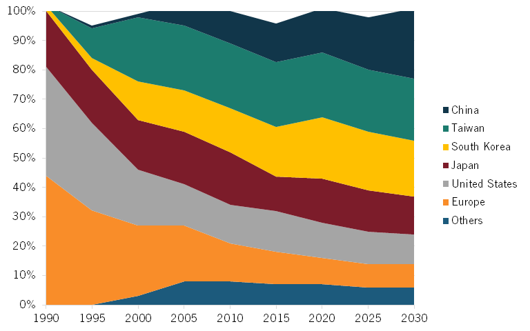
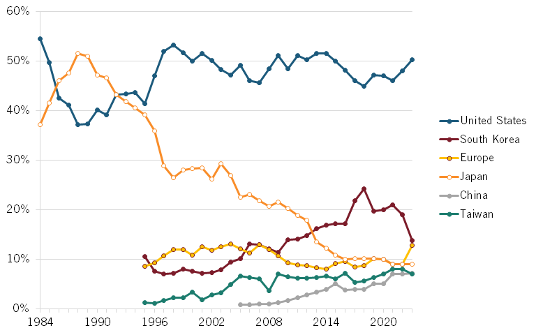
From 1990 to 2021, the U.S. share of global semiconductor production fell by 70 percent, from 37 percent to 12 percent.
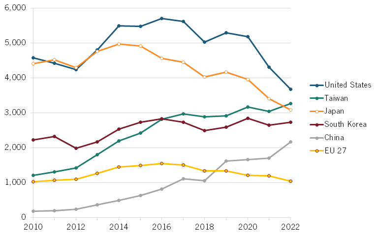
U.S. enterprises continue to lead the world in semiconductor design (e.g., AMD, Apple, Qualcomm, etc.), and are highly competitive in semiconductor manufacturing (e.g., Intel and Micron) and SME tooling (e.g., Applied Materials, Lam Research, etc.) Indeed, as the Australian Strategic Policy Institute (ASPI) wrote, “The US excels in the design and development of the most advanced semiconductor chips and has a research lead in the technology areas of high performance computing and advanced integrated circuit design and fabrication.” [18] However, while the emergence of the fabless chip design ecosystem has preserved America’s leading revenue share in the global semiconductor industry, where the United States has severely faltered is in its extent of semiconductor manufacturing. In fact, from 1990 to 2021, the U.S. share of global semiconductor production fell by 70 percent, from 37 percent to 12 percent. [19] Conversely, over that time, China’s share rose from virtually nil to 12 percent. (See figure 2.)
Figure 2: Global semiconductor manufacturing capacity, 1990–2030 forecastFigure 20
The significantly declining U.S. share of global semiconductor manufacturing activity was the catalyst for America’s major recommitment to revitalizing the competitiveness of its semiconductor industry when Congress passed, and the Biden administration signed, the 2022 CHIPS and Science Act. The legislation authorized a 25 percent investment tax credit (ITC) and appropriated $52.7 billion to support the industry, including $11 billion for R&D activities and $39 billion for a “CHIPS for America Fund” to bolster U.S. semiconductor manufacturing by providing financial incentives for building, expanding, and equipping domestic fabrication facilities.[21] The United States (like Europe) seeks to double its share of global semiconductor manufacturing activity over the coming decade—objectives that will abut China’s efforts to also similarly increase its share in the years ahead.[22] That U.S. semiconductor companies depend on the Chinese market for 36 percent of their sales represents a significant concern as China seeks to grow its domestic industry in a quest for autarkic self-sufficiency.[23]
Overview of China’s Semiconductor Industry
As noted, China lags behind the global innovation frontier in most aspects of semiconductor design and fabrication, including with regard to key inputs such as EDA software and lithography equipment. However, Chinese enterprises such as Huawei’s HiSilicon and Biren have innovated increasingly competitive logic chips, especially those powering mobile devices and graphical processing units (GPUs) servicing AI applications. China has also demonstrated an ability to cost-effectively manufacture less-technologically complex mature-node logic chips. Chinese memory chip manufacturers Yangtze Memory Technologies Co. (YMTC) and ChangXin Memory Technologies (CXMT) seemed to be making significant strides up until about 2020, but appear to have fallen off the innovation pace relative to global leaders since.
Nevertheless, China is rapidly closing the gap across many facets of the semiconductor production process and is developing genuine IP and innovation capabilities across the board. In January 2024, Intel CEO Pat Gelsinger asserted that, despite China’s ongoing efforts to advance its semiconductor industry and design more sophisticated chip manufacturing tools, the country still lags behind the global semiconductor industry by approximately 10 years.24 While there’s no question that China’s behind, the real gap, as noted, is probably half that now, or about five years—at least for the design and fabrication of leading-edge logic chips. China continues to plough hundreds of billions of dollars into its semiconductor industry in an effort to close that gap. Moreover, over the long term, as one observer commented, “The likelihood of China developing advanced chip-making capabilities is almost certain.”25
China is rapidly closing the gap across many facets of the semiconductor production process and is developing genuine IP and innovation capabilities across the board.
Ever since the 2013 Third Party Plenum, the Chinese government “has made semiconductors the country’s top industrial innovation priority.” [26] China’s “2014 National Guidelines for Development and Promotion of the IC Industry” (often called the “National IC Strategy”) called for $150 billion in investments to establish a fully “closed-loop” semiconductor ecosystem in China. The plan unabashedly called for eliminating China’s trade deficit in ICs by 2030 and making China the world’s leader in IC manufacturing by then. [27] In 2015, China released its “Made in China 2025” (MIC 2025) strategy, which refined some of these targets, setting a goal of achieving 40 percent self-sufficiency in semiconductors by 2020 and 70 percent by 2025. [28] In reality, China is likely to only achieve 30 percent self-sufficiency by the end of 2025. [29] RAND’s Jimmy Goodrich has noted that China would probably need to invest at least an additional $1 trillion more to achieve true self-sufficiency in the industry. [30]
Nevertheless, these strategies make clear that China recognizes that semiconductors represent a foundational technology that underpins its economic and national security wherewithal, and that the country is willing to undertake the long-term investments necessary to reach its goal of achieving self-sufficiency and reducing dependence on foreign technologies in this critical sector. As Goodrich explained, “Semiconductors are integral to China’s goal of developing a complete industrial system. This means having capability up and down the supply chain, with the goal that, in the event of a conflict, China can sustain its industrial system and its economy.”[
](#_edn31)
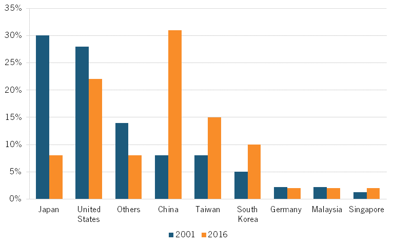
China’s efforts have paid dividends. For instance, from 2001 to 2016, China’s share of global value added in the semiconductor industry grew almost fourfold, from 8 to 31 percent, while the United States’ share fell from 28 to 22 percent, and Japan’s share fell by over two-thirds, from 30 to 8 percent. (See figure 3.)
Figure 3: Country share of value added in global semiconductor industry[32]
Nevertheless, according to data from the Semiconductor Industry Association (SIA), considering global semiconductor industry market share, China commanded only 7.2 percent of the global market in 2023, compared with 7 percent for Taiwan, 9 percent for Japan, 12.7 percent for the EU, 18.8 percent for South Korea, and 50.2 percent for the United States. (See figure 4.)
Figure 4: Global semiconductor industry sales market share by nationally headquartered companies[33]
Despite the significant decline in the share of global semiconductor manufacturing the United States has experienced, it has maintained its leadership in overall global semiconductor market share thanks especially to its strengths in EDA and semiconductor design as well as to world-leading companies in the logic, memory, and analog market segments.
Japan, once the world leader in semiconductors, has experienced significant decline over the past three decades. Since 1988, Japan has gone from holding 52 percent of the semiconductor market share to just 7 percent, a decrease of 87 percent. This major decline can be attributed to an inability or unwillingness of Japanese firms to adapt during the 1990s and early 2000s as other significant semiconductor foundries were established. This lack of innovation, research, and development, coupled with falling Japanese electronics sales, made adaptation and competition in the semiconductor industry difficult for legacy Japanese companies.[34]
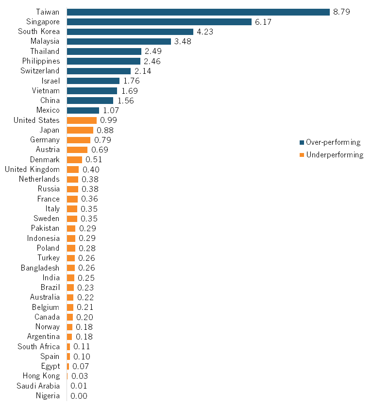
One of these new semiconductor manufacturers founded during the 1990s was TSMC. Now the largest manufacturer of semiconductors in the world, TSMC produces the majority of semiconductors made in Taiwan. The semiconductor industry accounts for 15 percent of Taiwan’s gross domestic product (GDP) while producing 60 percent of the world’s semiconductor chips, a large percentage of which are highly advanced.35 Though Taiwan accounts for just a small share of the global market (7 percent), its output relative to its size makes Taiwan the strongest relative performer. This can be seen using location quotient (LQ) information from ITIF’s Hamilton Index, which assessed 10 strategically important industries. An LQ is calculated as a country’s share of global output in an industry divided by the country’s overall share of the global economy.36
Figure 5 shows LQ data for the Hamilton Index category of the computers and electronics industry, a strategically important industry that includes semiconductors. Taiwan tops the list with an LQ of 8.79, exceeding close competitors such as South Korea and Singapore with LQs of 6.17 and 4.23, respectively. With LQs greater than 1, all three countries are overperforming, producing an output in the computer and electronics industry greater than the global average. China’s LQ of 1.56 means that the computers and electronics industry contributes 50 percent more to China’s economy than it contributes to the global economy. The United States’ LQ of 0.99 means that the computers and electronics industry contributes about as much to the U.S. economy as it contributes relatively to the global economy. Japan lags behind here with an LQ of 0.88. (See figure 5.)
Figure 5: Relative performance in computers and electronics industries[37]
SubSector Analysis of China’s Semiconductor Industry
This section analyzes China’s innovativeness by industry subsector, considering China’s strengths in EDA, semiconductor design and fabrication—of leading-edge and mature node logic chips, and memory chips—as well as the semiconductor ATP and SME/tooling sectors.
Electronic Design Automation
EDA refers to the software, hardware, and services that assist in the definition, planning, design, implementation, verification, and subsequent manufacturing of semiconductors.38 Historically, EDA has “constitute[d] a weak link in the PRC’s efforts to build a leading domestic semiconductor value chain.”39 As such, China has targeted progress in EDA since MIC 2025 and the 14th Five Year Plan, with the efforts now “logging some initial successes.”40
In March 2023, Huawei announced that it had achieved a number of breakthroughs in the development of EDA software, which it suggested would free China’s industry from reliance on foreign suppliers of those tools when producing semiconductors of 14 nm or more.[41] Huawei claimed it had substituted 78 (foreign) software and hardware items over the previous three years.[42] These breakthroughs likely came in partnership with Beijing-based Empyrean Technology, China’s leading EDA player. Empyrean claimed last year that it could fully support 7 nm digital processes and 5 nm analog processes.[43]
Beyond Empyrean, other leading Chinese EDA companies include GWX Technology, Primarius, Semitronix, Shenzhen Giga Design Automation, UniVista, and X-EPIC.[44] By 2020, Chinese companies had captured 11.5 percent of the domestic EDA market (up from 6.2 percent in 2018), with that share expected to increase to 14 percent by 2025.[45]
In June 2023, in Nanjing, China, Southeast University launched a National EDA Innovation Center, the first national technology innovation center in China dedicated to IC design (and which had been under development since September 2020). Yang Jun, a professor at Southeast University tasked with leading the center, noted its mission would be to “undertake the critical work of breaking the United States’ chokehold in EDA software,” not just for mature-node chips, but also ultimately for advanced chips including gate-all-around (GAA) transistors, which the United States has subjected to export controls.[
46 ](#_edn46) The Center is coordinating the work of multiple laboratories, facilitating the establishment of an independent EDA ecosystem by coordinating the participation of companies such as Empyrean, and promoting EDA competitions, such as the Integrated Circuit EDA Elite Challenge, with the goal of “increasing domestic market share of Chinese EDA players.”[
47 ](#_edn47)
Despite the progress, Chinese EDA enterprises have a long way to go, and even Empyrean in a recent prospectus noted that it “could not yet cover the full digital circuit process on its own.” [48] Observers believe that “it is more likely in the medium term that the PRC will make headway in EDA tools for processes at the 14 nm level or above.” [49]
Design and Fabrication
Semiconductor chip design and semiconductor fabrication are clearly separate steps in the semiconductor production process (and ordinarily would be evaluated separately), but since China’s progress in one is so intimately linked to its progress in the other, this section will consider both largely simultaneously, but segment by advanced-node and mature-node logic chips and then memory.
Semiconductor Design
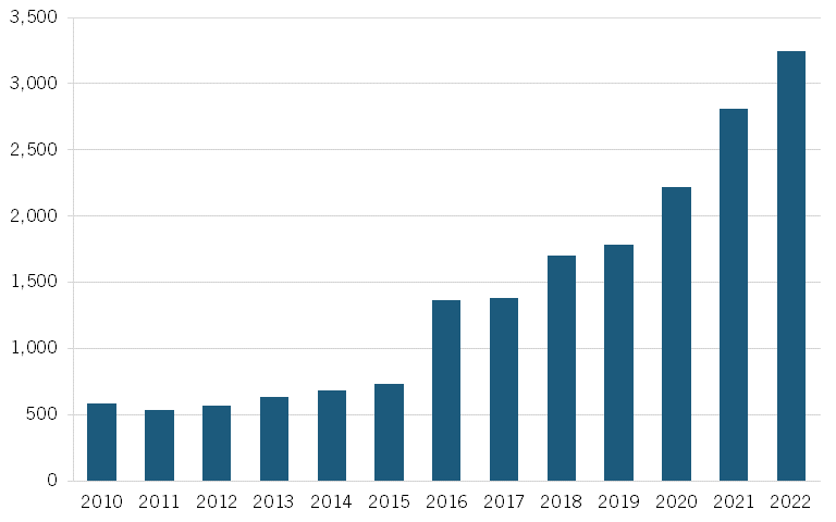
As one report notes, “China’s design industry has rapidly increased in size since 2015, driven by factors such as the widespread availability of capital (including from both the government and private sector), government support, a desire to localize the industry, demand growth, the acquisition of foreign firms, and downstream users designing their own semiconductors.” [50] In fact, from 2010 to 2022, the number of semiconductor design firms in China increased nearly sixfold, from 582 to 3,243. (See figure 6.) The Chinese IC design industry’s total sales reached 557.4 billion yuan ($76.7 billion) in 2023. [51] Still, Chinese design firms accounted for only 8 percent of global design revenue in 2022, with no Chinese firms among the top 25 global design firms. [52]
Figure 6: Number of semiconductor design firms in ChinaFigure 53
RISC-V is an open-source instruction set architecture used to develop custom processors for a variety of applications, from embedded designs to supercomputers.[54] RISC-V essentially represents a set of computing standards that provide a common language for designing the processors found in devices such as smartphones, tablets, and Wi-Fi routers.[55]
China is actively embracing and innovating with RISC-V technology.[56] And as industry analyst Paul Triolo wrote, “[E]ager to wean Chinese firms off proprietary Western chip IP and architectures, such as x86 and Arm, Beijing is also fully supporting the development of the RISC-V reduced instruction set architecture. Chinese officials, and industry leaders such as Alibaba and its chip-design arm T-Head, have embraced the RISC-V approach over the past three years.”[57] Indeed, more than 100 “significant” Chinese companies are designing chips with RISC-V today, as are at least 100 more start-ups, according to industry analyst Handel Jones.[58] The top 10 RISC-V star-tups in China have secured funding totaling over $1 billion.[59] As one report notes, while many RISC-V “applications are in fairly mundane consumer products,” engineers believe “the technology will eventually take over more demanding tasks.”[60] For example, on November 24, 2023, DAMO Academy (Alibaba’s research division) unveiled three RISC-V-based processors. Elsewhere, “Chinese aerospace scientists have proposed using RISC-V to develop high-performance spaceborne computers,” while Alibaba’s T-Head has designed a RISC-V chip to operate a cloud-styled computing service.[61]
Advanced-Node Logic Chips
As The Economist wrote, “China’s chip industry [remains] far from the technological frontier. Even if Huawei and SMIC eventually succeed at producing 5nm chips, they will remain well behind Samsung, a South Korean tech giant, and TSMC, a Taiwanese foundry, both of which began mass-producing 3nm chips as far back as 2022.” [62] As G. Dan Hutcheson, vice chair of research firm TechInsights, explained, “Ten years ago, [Chinese companies] were two generations behind. Five years ago, they were two generations behind, and now they’re still two generations behind.” [63] However, this doesn’t mean China isn’t making considerable progress in certain pockets.
In August 2023, Huawei released the Mate 60 Pro smartphone, shown, which deployed the 7 nm Kirin 9000S chip and which was manufactured by SMIC using its SMIC N+2 process technology.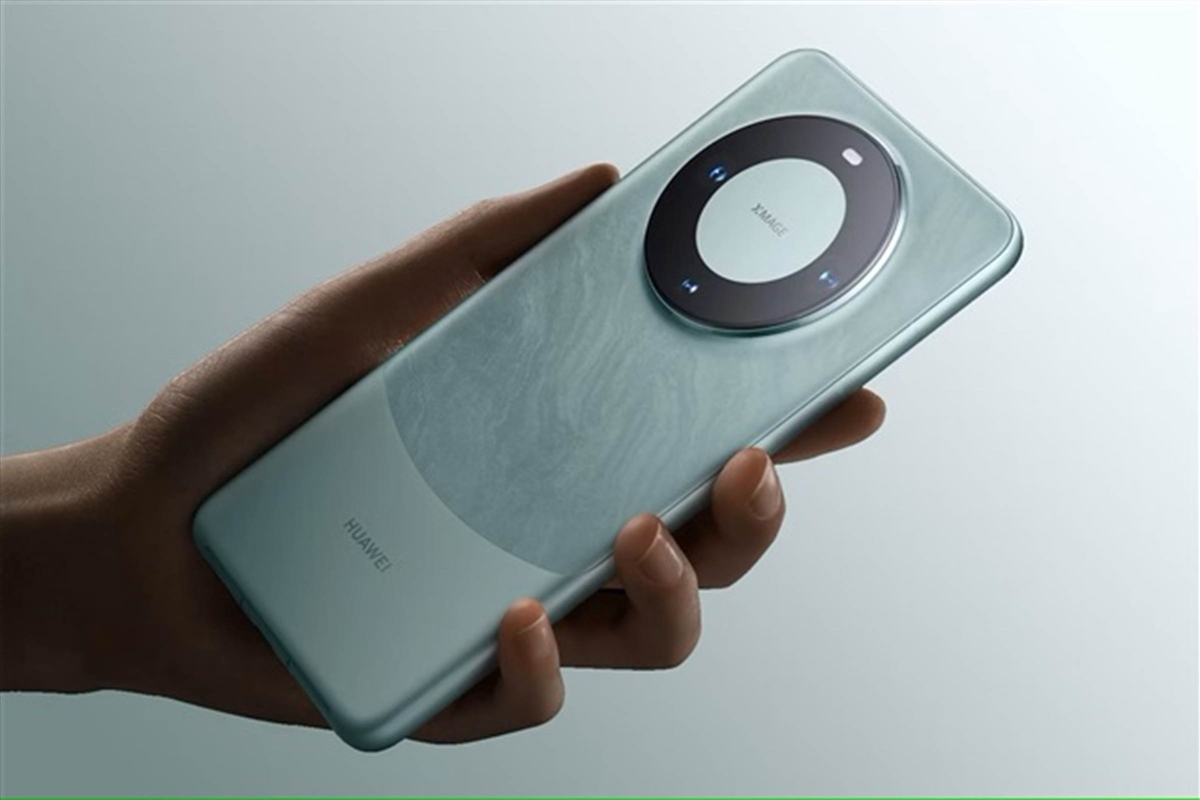
For instance, in August 2023, Huawei released the Mate 60 Pro smartphone, which deployed the 7 nm Kirin 9000S chip (which Huawei’s HiSilicon design arm architected) and which was manufactured by SMIC using its SMIC N+2 process technology “with capabilities that shocked the world in terms of its performance.” [64] As Dylan Patel of SemiAnalysis and Doug O’Loughlin of Fabricated Knowledge commented, “Comparing the MatePro’s [chip] to Qualcomm’s chip, made by Samsung, it is probably only 18 months behind and in some respects it’s actually just as good. … People didn’t think China would be capable of producing this.” [65]
Patel and O’Loughlin observed that the Mate Pro’s network performance (upload/download) speeds were on par with that provided by Qualcomm’s chips (and probably superior to those of the latest iPhone) and that its GPU/AI features (supporting phone features such as gaming, videos, and cameras) were mostly on par with those of competitors."66" They commented that “it’s a really good chip, with both hands tied behind their back [meaning it was manufactured without leading-edge EUV lithography equipment, but with older DUV equipment]” and “at worst it’s 18 months behind [global leading edge].”"67" As Patel concluded:
Put simply, [the] Kirin 9000S is a better designed chip than the West realizes. It has solid power and performance. Even with the lackluster export controls, this is a leading edge chip that would be near the front of the pack in 2021, yet was done with no access to EUV, no access to cutting edge US IP, and intentionally hampered. We cannot overstate how scary this is.[68]
Because SMIC could not make Huawei’s Kirin processor using the latest EUV equipment due to the aforementioned export controls, it used existing DUV equipment it possessed (pre-export controls) to employ a technique called “double patterning”—a process that uses multiple laser passes to etch IC designs at sub-20 nm resolutions—to manufacture at 7 nm.[69] However, this process is time consuming and expensive, making it difficult to manufacture using this process at volume scale, which explains why analysts expected Huawei to ship only 7 million of the MatePro phones in 2023, and perhaps 40 million in 2024.[70] Nevertheless, Patel has contended that SMIC’s N+2 process represents a “real, high volume production process technology” with strong yields.[71]
The SAQP case reflects that Chinese semiconductor developers are attempting to be as innovative as they can possibly be at process innovation, at least with the assets and technologies available, even if these are clearly behind the global frontier currently.
On Friday, March 22, 2024, Huawei (presumably with SMIC) announced that it had filed for patents for a technology called “self-aligned quadruple patterning,” or SAQP: a technique for etching lines on silicon wafers multiple times to increase transistor density.72 The SAQP method described in Huawei’s patent application involves etching lines on silicon wafers multiple times to boost transistor density, reduce power consumption, and potentially increase performance.73 Already, SiCarrier, a Chinese state-backed chipmaking developer, had been issued a SAQP-related patent in late 2023 that illustrates how to employ DUV and SAQP processes to achieve certain technical thresholds evident on 5 nm chips. The SAQP technology represents a similar approach to one Intel explored when looking to move to sub-10 nm processes, but as Anton Shilov wrote, “In the Huawei and SMIC case, quadruple patterning is the only technique that increases transistor density using the tools that the contract chipmaker already has.”74 In other words, the case reflects that Chinese semiconductor developers are attempting to be as innovative as they can possibly be in process innovation, at least with the assets and technologies available, even if these are clearly behind the global frontier currently. It’s also evidence that China is trying to reach a state of “good enough” to have sufficient domestic technologies to produce information communications and telecommunications (ICT) goods servicing domestic markets.
SMIC is currently developing its SMIC N+3 “5 nm” process that should feature 130 million transistors per square millimeter (mm^2). As Patel has written, “If nothing changes with current restrictions, we expect Huawei and SMIC to have a true 5nm-based chip in 2025 or 2026 with large scale AI chips not so long after.” [75] Ultimately, Patel has argued that “SMIC is at most only a few years behind Intel and Samsung” and “at worst only a handful years behind TSMC.” [76] However, as noted, most analysts would peg this gap at closer to five than just a couple years.
Elsewhere, a plethora of Chinese competitors are designing AI chips, including Huawei (with its Ascend chip), Biren, Tencent, Alibaba, Baidu, and MetaX. Patel has asserted that these firms “will soon be able to deliver on chips that are on par with Nvidia’s A100 [using] SMIC 7nm in 2 years at significant volumes.”[77] Commenting on Huawei’s Ascend GPU chips, one observer (requesting anonymity) noted that Huawei’s highest-end product is likely comparable to an NVIDIA H800 in most features save for energy efficiency. Huawei has developed a proprietary software platform, called “CANN,” that helps developers use its chips to build AI models.
In the GPU space, Biren Technology’s BR100 processor competes in the market against NVIDIA’s H100. The H100 features 80 billion transistors on the TSMC N4 process node whereas the BR100 is only 3 billion transistors behind the 7 nm process node.[78] Hong Zhou, cofounder and CTO of Biren Technology, asserts that the BR100’s architecture optimizes the data flow in depth, solving the bottleneck of data migration and insufficient parallelism through six technical characteristics, which means the BR100 chip has “achieved leapfrog progress” in performance and energy efficiency.[79] While the BR100 delivers powerful performance speeds, industry observers note that NVIDIA’s CUDA ecosystem, which tightly integrates hardware and software, is likely more attractive and has made NVIDIA an essential partner for developers and researchers.[80]
Chinese central processing unit (CPU) chipmaker Loongson recently launched its new 3B600 and 3B700 processors, which the company claims match Intel’s 10th-generation chips in single-core performance.[81] The company claims its latest iterations have seen up to a 20-fold gain in single-core capabilities, though company vice president Zhang Ge admits the company’s “chips lag mainstream offerings for multi-core” processors.[82] Nevertheless, China’s government is eyeing the company’s homegrown solutions as attractive offerings for the country’s lucrative education and government markets. Elsewhere, Wuhan Xinxin is building a factory that will be able to produce 3,000 12-inch high-bandwidth memory (HBM) wafers a month to expand China’s domestic base of AI-capable microchips.[83]
Larger-Node Chips
As noted, larger-node chips, also known as legacy or mature chips, are 28 nm in size or larger.Legacy chips But as one report notes, “Despite the name, legacy chips are not stale technology. The connotations associated with terms like ‘mature,’ ‘older,’ and ‘legacy’ are misleading because these categories of chips are constantly being refined for new requirements and applications.”Another report Rather, larger-node chips are foundational to many markets, including the industrial, aerospace, and defense sectors. Innovations in these chips include the use of wide bandgap materials such as silicone carbide (SiC) and gallium nitrate (GaN), important in clean energy applications. Elsewhere, as one commentator noted, “The main innovation for the auto industry is happening on mature nodes. They need to be very energy efficient and safe.”Commentary
China is likely to become an ever-more significant player in this sector of the market, but its basis for competitive advantage here is likely to be more predicated on massive scale (supported by large, state-driven industrial subsidization) that facilitates price-driven, not innovation-driven, competition.87
China will add more chipmaking capacity than the rest of the world combined in 2024, with 1 million more wafers a month than in 2023.
China will account for the most significant share of new semiconductor capacity coming online over the next several years. Indeed, analysts expect that China will add more chipmaking capacity than the rest of the world combined in 2024, with 1 million more wafers a month than in 2023. China’s share of global mature-node production is expected to grow from 31 percent in 2023 to 39 percent in 2027.[88] China currently commands 27 percent of global production capacity for chips in the 20–45 nm range, and 30 percent of global production capacity in the 50–180 nm range. Moreover, analysts expect China to build the most new fabs or major expansions in the 2022 to 2026 time period, with China bringing 26 new facilities online, and Taiwan 19. (See figure 7.) China’s IC output surged 40 percent to 98.1 billion units in the first quarter of 2024, driven primarily by production of legacy chips.[89]
Figure 7: New fabs and major expansions expected to come online, 2022–2026[90]
The growth of China’s semiconductor industry—especially in the legacy chip segment—has been driven considerably by massive industrial subsidization designed to help its companies reach economies of scale in production. Thus, as one report notes, “Chinese firms—supported by lower costs in China due to government subsidies and other factors—are able to offer significantly lower prices.” [91] For instance, China’s microcontroller processor manufacturer Giga Device was offering its products at prices that were 20 to more than 30 percent lower than non-Chinese competitors, such as the French firm ST Microelectronics, across most of 2022 and 2023. [92] Chinese subsidies allow Chinese semiconductor firms to compete in markets without having to earn market-based rates of return, and thus they can sell their products at much lower prices, which places firms that do have to earn market-based rates of return at a significant disadvantage while also disrupting the economics of innovation in the industry, as companies depend on the profits from one generation of semiconductor products to finance the R&D expenses that go into innovating the next generation. This has been a significant challenge for global memory chip manufacturers as well—and this dynamic threatens to extend to every semiconductor subsector which China aggressively subsidizes.
China’s aggressive subsidization of larger-node chips contributes to overcapacity, artificially lowers prices, and disadvantages firms that must earn market-based rates of return, significantly disrupting the economics of innovation in the global semiconductor industry, with deleterious downstream ramifications not just for mature-node chipmakers, but for chipmakers at all node sizes.
Memory Chips
The semiconductor memory industry has long been a strategic priority for China’s economic development.93 YMTC, China’s leading NAND maker, is a Chinese state-controlled joint venture launched by the National IC Industry Investment Fund, the erstwhile state university-controlled fabless semiconductor firm Tsinghua Unigroup, and the Hubei Science and Technology Investment Group, supported by $24 billion in initial government funding allocated for its initial Wuhan factory alone.94 Launched in 2017, CMXT is another Chinese-government-created semiconductor manufacturer, focusing on DRAM technology. CMXT was established as a project co-led by the local state-owned Hefei Industrial Investment Fund (HIIF) and GigaDevice Semiconductor Beijing (a Chinese designer of flash memory chips), with HIIF kicking in $8 billion to launch the effort.95
China’s aggressive subsidization of larger-node chips contributes to overcapacity, artificially lowers prices, and disadvantages firms that must earn market-based rates of return, significantly disrupting the economics of innovation in the semiconductor industry.
As Triolo wrote, “Memory is a very different sector than logic, highly commoditized and competitive, with no legacy nodes, requiring companies to constantly upgrade toward the most advanced processes.” [96] As he noted, “YMTC had moved rapidly up the NAND manufacturing curve, producing 128-layer NAND and moving rapidly toward more advanced processes, at 232 layers and above.” [97] A TechInsights article finds that YMTC introduced “the first 200+ layer 3D NAND Flash” on the market, ahead of rivals Samsung, SK Hynix, and Micron. [98] YMTC grew incredibly fast after its launch, reaching 5 percent of global market share by 2021, on a track to surpass 10 percent by 2027. [99] In 2022, Apple considered acquiring YMTC’s NAND memory chips for use in iPhones and iPads to be sold in China, and reportedly wanted to increase the order up to 40 percent of the chips required for all iPhones. [100] However, in December 2022, the U.S. Department of Commerce’s Bureau of Industry Security (BIS) added YMTC to its “Entity List”—a trade “blacklist” that subjects listed entities to export licensing requirements—and this action appears to have significantly stymied the company’s progress. In the months that followed, YMTC laid off 10 percent of its staff and reduced its equipment procurement and expansion plans. [101]
For its part, CXMT has became the workhorse DRAM company in China, but “the company faces significant challenges in the execution of its roadmap” and analysts don’t regard it as competing at the leading edge.[102] The company is “racing to produce China’s first domestic high bandwidth memory, a critical component in artificial intelligence computing.”[103] However, as Counterpoint research semiconductor analyst Dan Wang noted, “When your DRAM technology already lags behind global rivals, that puts your HBM technology at a disadvantage to be competitive in a fully commercial market … It’s not that easy for China’s national champion to break the international dominance in the sector. Its primary objective remains fulfilling China’s domestic demand.”[104]
Ultimately, as Triolo noted, while “key players like memory makers YMTC and CXMT [are] hobbled by lack of access to cutting-edge tools, [they are] still capable of producing useable memory” [105] In fact, TrendForce projects that the Chinese industry’s share of the NAND flash market will have peaked at 31 percent in 2023 before declining to 18 percent by 2024, while its share of the global DRAM market will fall from 15 percent in 2022 to 12 percent by 2025. [106] Nori Chiou, an investment director at White Oak Capital and a former analyst who looked at the IT sector, estimates that Chinese chipmakers lag their global rivals by a decade in HBM. [107] To be sure, YMTC (like CXMT) has shown itself to be an innovative firm; however, its lack of access to advanced tooling raises questions as to whether it can maintain its innovative wherewithal.
Semiconductor Manufacturing Equipment
Lithography represents a crucial step in the chipmaking process, wherein a chip wafer gets inserted into a lithography machine and exposed to DUV or EUV light and a pattern is printed onto a chip’s resist layer through a photomask. In the subsequent process step, “etching,” the wafer is baked and developed, and some of the resist layer is washed away to reveal a 3D pattern of open channels.[108] The essential point is that the lithography process determines just how small the transistors on a chip can be, which is why lithography innovations have been every bit as foundational as those in design to moving the industry toward lower process nodes.
As such, catching up in lithography has long been a central focus of China’s chip aspirations, with the efforts going back to China’s “Project 02” launched in 2008, called “The Project of Manufacturing Complete Sets of Technology for Very Large Integrated Circuits.” [109] Despite these efforts, as Triolo wrote, “Chinese lithography companies appear to be years behind industry leader ASML and Japanese firms such as Nikon and Canon, making lithography one of the critical technology bottlenecks.” [110] For this reason, Triolo observed that “officials in Beijing are developing new approaches to public-private collaboration to push innovation on key technologies, such as advanced lithography … easing the transfer of advanced state-backed R&D to designated private sector companies, by pushing companies to work together on critical technologies, and by pursuing approaches that have been successful in other sectors.” [111]
Shanghai Micro Electronics Equipment (SMEE) Group, China’s leading lithography developer, claimed in December 2023 to have successfully developed a 28 nm lithography machine, the SSA/800-10W.[112] (By comparison, TSMC was manufacturing 28 nm chips by 2011, and Intel was by at least 2014. Intel and TSMC are now, or imminently about to be, delivering chips at the 2 nm or even sub-2 nm level.)[113] Nevertheless, as one observer commented, “This advancement represents a major leap in China’s quest to close the technological gap in the global chip industry.”[114]Despite the claimed breakthrough, analysts have raised questions about how long it will take SMEE to produce such machines in bulk. SMEE’s current SSA600 series can utilize 90 nm, 110 nm, and 280 nm processes.
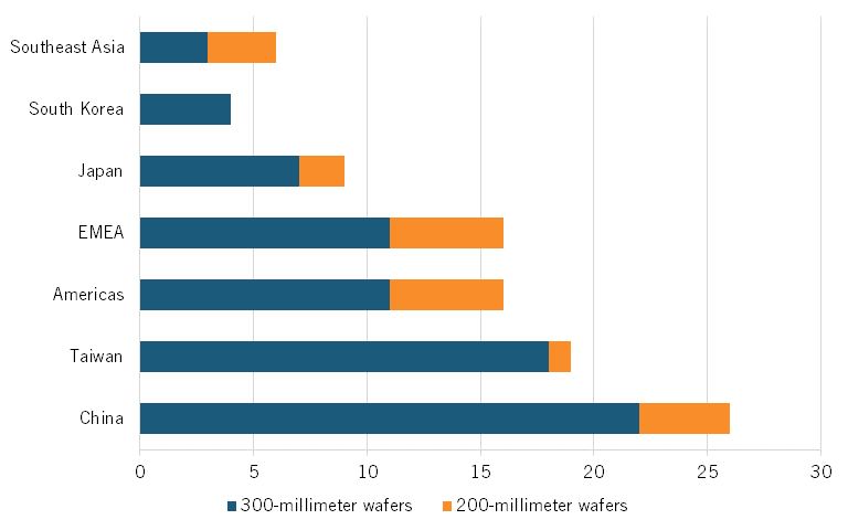
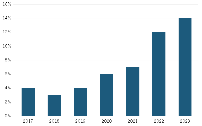
Naura Technology Group represents China’s largest chip production equipment manufacturer, its tooling focused on the etching process, followed by AMEC, which makes deposition equipment. Overall, the domestic market share of Chinese producers of wafer-fabrication tools rose from 4 percent in 2019 to an estimated 14 percent in 2023. (See figure 8.)
Figure 8: Chinese chip-fabrication equipment makers’ share of Chinese market [115]
Semiconductor Assembly, Test, and Packaging
After front-end chip fabrication, wafers are typically sent to other facilities for back-end manufacturing activities such as ATP. At this step, chips are cut from the silicon wafer, tested for performance, and packaged to protect the chip and allow for its integration into finished electronic devices by attaching electrical interconnections.116 Semiconductor ATP generally occurs through one of two business models: 1) as in-house ATP services performed by IDMs and foundries after fabrication, or 2) by outsourced assembly and test (OSAT) firms, which perform ATP activities for third-party customers.117
Figure 9: Number of ATP facilities per country/region, 2021[118]
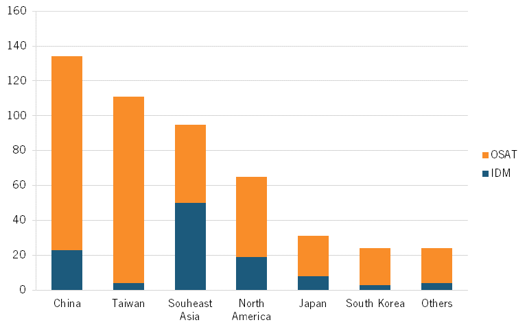
As of 2021, China accounted for 27 percent (134) of the world’s 484 ATP facilities. (See figure 9.) By August 2023, Chinese ATP firms commanded 38 percent of the market, with the five largest OSAT players—JCET, HT-Tch, TF, LCSP, and Chippacking—all being Chinese.[119]
ATP has historically been viewed as labor intensive and lower value added than design and fabrication, explaining why, historically, firms have set up ATP facilities to a larger extent in developing countries.[120] However, one observer noted that “packaging is the new pillar of innovation in the semiconductor industry—it will change the industry dramatically” as new technologies enable chips to be combined and stacked, and their performance enhanced.[121] Packaging matters for the kind of high-power semiconductors needed for AI applications. Indeed, a shortage of a particular type of packaging known as Chip on Wafer on Substrate, or CoWoS, has been a key bottleneck in the production of Nvidia Corp’s AI chips.[122]
Indeed, as Triolo noted, “Packaging is now becoming a key part of overall production, with back-end packaging being designed into the entire production process, from EDA tools, to integration of IP from companies such as ARM, to 3-d packaging designs that enable greater functionality with a mix of semiconductors at different levels of complexity.” [123] He further observed, “When it comes to design and packaging, some Chinese firms are using chiplet design already, which is a design approach that integrates chips produced using different processes on one substrate, along with advanced packaging technologies, including 2.5- and 3-d packaging.” [124]
However, industry observers at an ITIF roundtable contended that “while China has made some progress, it really doesn’t have that capability on the leading edge” of semiconductor ATP.[125]
Advanced Semiconductor Research
Chinese researchers stand at the forefront of innovating some semiconductor technologies, although the question is the extent to which these can be commercialized and scaled by industry. For instance, Professor Liu Kaihui of Peking University has developed new wafers for semiconductors that are just one atom thick (thereby termed “2D”). These new 30.5 centimeter wafers are thinner and more efficient and could “cheaply and potentially revolutionize the semiconductor industry,” its creators claim."126" Elsewhere, researchers from China and the United States have jointly created a new type of stable semiconductor graphene, which exhibits performance 10 times higher than silicon and 20 times larger than the performance of the other two-dimensional semiconductors."127"
China’s semiconductor industry is not nearly as R&D-intensive as other leading nations’ semiconductor sectors.
In March 2024, at the IEEE International Solid-State Circuits Conference in San Francisco, Professor Zhou Jun and his team from the University of Electronic Science and Technology of China (UESTC) unveiled what’s been billed as “the world’s most energy-efficient AI chips for mobile devices.” [128] The chips’ design leverages a novel architecture that addresses AI chips’ thirst for power through multiple optimizations, including dynamic computation engines, an adaptive noise suppression circuit, and an integrated keyword and speaker recognition circuit. A UESTC press release noted, “The chip achieves a recognition energy consumption of less than two microjoules per instance, with an accuracy rate exceeding 95 per cent in quiet scenes and 90 per cent in noisy environments, setting new global benchmarks for both energy efficiency and accuracy.” [129] At the conference, the UESTC team also unveiled a chip that helps detect seizures in individuals with epilepsy that achieved a detection accuracy rate of over 98 percent. [130]
In July 2024, Chinese scientists announced development of what could be the fastest analogue-to-digital converter (ADC) for military use. The device can reduce the time delay of electronic warfare receivers from nanoseconds to picoseconds, or one-trillionth of a second. The chip technology would make radar signal detection and responses 91.5 percent faster than currently deployed technologies, nearly doubling the speed of combat to potentially give the Chinese military a critical edge. The chip is based on mature 28 nm process technology."131"
Analysis of Innovation Inputs to China’s Semiconductor Sector
This section examines indicators assessing China’s semiconductor competitiveness at the industry level, considering such factors as R&D intensity, scientific publications, and patenting levels.
R&D Intensity
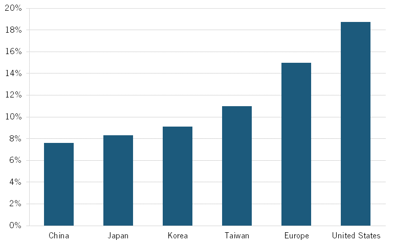
Broadly, China’s semiconductor industry is not nearly as R&D-intensive as other leading nations’ semiconductor sectors. In fact, in 2022, China’s semiconductor-sector R&D intensity of 7.6 percent was just 40 percent of America’s 18.8 percent, and well below the EU-country average of 15 percent, or Taiwan’s 11 percent (South Korea and Japan recorded R&D intensities of 9.1 and 8.3 percent, respectively). [132] (See figure 10.) China’s 7.6 percent semiconductor-sector R&D intensity in 2022 was actually down slightly from the 8.4 percent it had invested in 2018. [133]
Figure 10: Select nations’ semiconductor industry R&D expenditures as a percentage of sales, 2022[134]
In terms of semiconductor companies’ levels of R&D investments (as reported in the “2023 EU Industrial R&D Investment Scoreboard”), Huawei led all Chinese semiconductor-related firms with an R&D intensity of 25.2 percent (although it produces a range of products beyond semiconductors), which was competitive though still below that of global leaders Intel, AMD, and MediaTek, which recorded R&D intensities of 29.6 percent, 25.9 percent, and 25.7 percent, respectively. (See Table 1.) Huawei was the only Chinese semiconductor company in the top 13 on this measure in the study.
Table 1: Leading semiconductor investors on the “2023 EU Industrial R&D Investment Scoreboard” [135]
Company
Headquarters
R&D Investment (Billions)
R&D Intensity
Intel
United States
€14.77
29.6%
AMD
United States
€5.40
25.9%
MediaTek
Taiwan
€3.34
25.7%
Huawei
China
€20.70
25.2%
Qualcomm
United States
€7.97
23.9%
Micron Technology
United States
€2.86
19.2%
NXP Semiconductors
The Netherlands
€2.17
17.8%
Broadcom
United States
€5.86
16.4%
ASML
The Netherlands
€4.04
14.4%
NVIDIA
United States
€7.99
14.2%
Analog Devices
United States
€1.51
14.2%
Scientific Publications
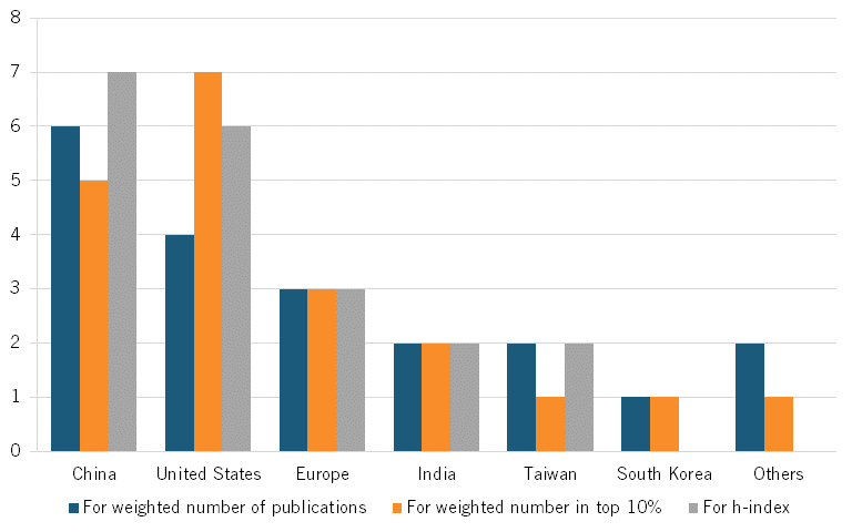
As noted, according to ASPI, “The US excels in the design and development of the most advanced semiconductor chips and has a research lead in the technology areas of … advanced integrated circuit design and fabrication.” [136] Nevertheless, Chinese researchers have made impressive strides in the number and quality of their scientific publications in semiconductors. Considering the h-index, a measure of the productivity and citation impact of scientific publications, China counts 7 institutions in the global top 20 research institutions releasing advanced IC and design publications. Specifically, the Chinese Academy of Sciences ranks 6th overall, followed by Peking University (8th), Huazhong University of Science & Technology (9th), Zhajang University (11th), Shanghai Jiaotong University (12th), Hong Kong University of Science and Technology (16th), and East China Normal University (20th). [137] China also places 6 academic institutions in the top 20 for the weighted number of publications on advanced IC design and fabrication, and 5 institutions for the weighted number of publications within the top 10 percent of highly cited publications. (See figure 11.)
Figure 11: Number of research institutions ranking among the top 20 institutions globally for their volume and quality of publications in advanced IC design and fabrication[138]
Patents
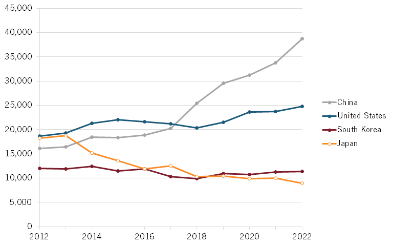
Scientific publications represent knowledge feedstock that can be turned into patent applications, and China has made tremendous strides in increasing its levels of semiconductor patent applications and semiconductor patents granted. In fact, in 2021–2022, 55 percent of global semiconductor patent applications (37,865) were Chinese in origin, more than doubling the 18,223 applications submitted by U.S.-based filers.[139] (See figure 14.) Chinese filers’ semiconductor patent applications doubled in number from 2012 to 2022.
Figure 12: Semiconductor patent applications, by country of origin[140]
While China has long been known for filing significant numbers of dubious patent applications—in part through incentives that compensate filers for submitting regardless of the applications’ merits—the evidence shows that it’s not simply fluff: Chinese entities are indeed receiving semiconductor patents in record numbers. The Patent Cooperation Treaty (PCT) allows for innovators to seek protection for an invention simultaneously in each of a large number of countries by filing an “international” patent application.[141] From 2010 to 2020, Chinese entities increased their levels of PCT semiconductor patents awarded nearly 30-fold (from 122 to 3,474), exceeding Japan’s count by 2020, while the number of patents being awarded to U.S. filers fell by 22 percent. (See figure 13.)
It is of note that while Japan is last among the countries examined here for semiconductor applications, they are second in patents granted. This could be attributed to the high quality of patents published in Japan in comparison with other countries. In 2020, Japan obtained 2,679 patent grants out of its 9,963 applications, a 27 percent grant rate. China, on the other hand, had just 11 percent of its patent applications granted. Unlike for China, Japanese filers likely apply for fewer potentially suspect patents, explaining its high ranking among semiconductor patent grant recipients.
Figure 13: Number of PCT patent grants in semiconductors[142]
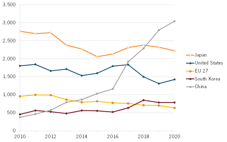 Considering IP5 patent family grants (referring to collective grants from the Chinese, European, Japanese, South Korean, and U.S. patent offices), China clocked in third for semiconductor patent family grants in 2020, with 2,335 issued, behind 3,645 for South Korean filers and 2,990 for Japanese ones.[143] China’s number of IP5 patent families in semiconductors increased nearly fivefold during the prior decade, from just 420 in 2010 to 2,335 in 2020, while Japan’s number fell by nearly 40 percent. (See figure 14.)
Figure 14: Number of IP5 patent families in semiconductors[144]
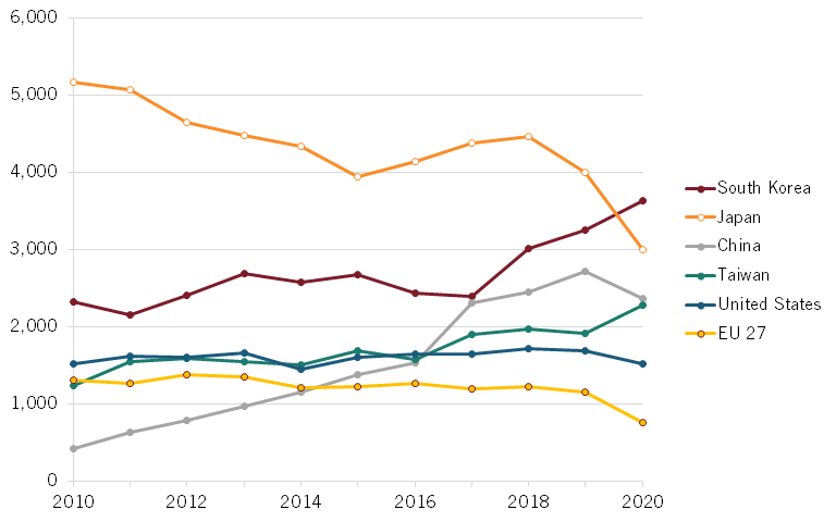
Figure 15: USPTO semiconductor utility patents granted[145]
Similar trends are apparent when considering semiconductor utility patents issued by the U.S. Patent and Trademark Office (USPTO). From 2010 to 2022, the number of patents USPTO issued to Chinese filers increased 12-fold, though China still trailed the United States and Japan (whose semiconductor patent levels were dropping) and Taiwan and South Korea (whose levels were gaining) over this time. (See figure 15.)
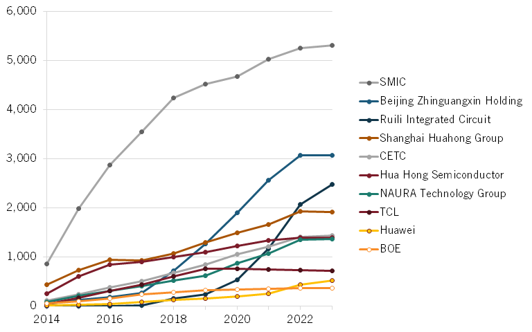
Over the past decade, the overall size of Chinese companies’ patent portfolios has correspondingly grown significantly. The size of SMIC’s patent portfolio increased from under 1,000 patents in 2014 to over 5,000 by 2023. (See figure 16.) Likewise, the number of patents held by Beijing Zhiguangxin Holding—which has assumed the holdings of the now defect Tsinghua Unigroup and spawned them into UNISOC, now China’s largest mobile phone chip designer—increased from just 7 to 4,632 over this time, while Huawei’s number of semiconductor patents increased from virtually nil to nearly 1,500.
Figure 16: Patent portfolio size of leading Chinese semiconductor companies[146]
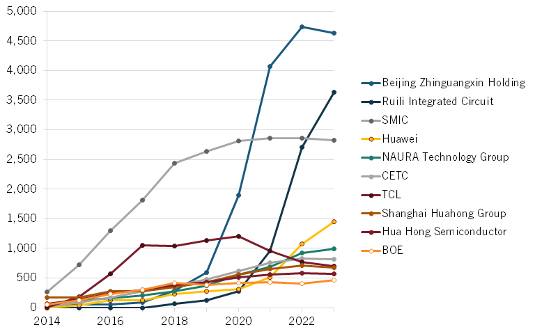
LexisNexis, an American data analytics company, has created a “PatentSight’s Patent Asset Index,” which seeks to evaluate the “competitive impact” of a company’s patent portfolio, doing so by multiplying the “technology relevance” of a patent, which is based on the number of citations a patent receives and its “market coverage,” which is based on the gross national income of the regions where the patent is protected."Patent Asset Index" Examining the “Semiconductor Device Manufacturing” category on the Patent Asset Index shows that Beijing Zhiguangxin Holding holds the strongest patents out of China’s top-10 largest semiconductor patent holders, followed by Ruili Integrated Circuit and SMIC. (See figure 17.) However, despite this growing strength, as one commentator noted, Beijing Zhiguangxin Holding represents only 2 percent of the total Semiconductor Device Manufacturing Index and “while there is a clear upward trend, it is major plyers like Samsung and TSMC that still hold the ‘lion’s share’ of the global semiconductor technology market.”"Semiconductor Device Manufacturing Index"
Figure 17: Top 10 Chinese semiconductor companies’ scores on the Patent Asset Index[149]
Company Case Studies
This section provides case study analyses of several Chinese semiconductor companies; they were selected randomly from Chinese semiconductor companies included in the “2023 EU Industrial R&D Investment Scoreboard” report.
Biren
Founded in September 2019 and headquartered in Shanghai, Biren Technology focuses on developing original general computing systems, establishing efficient software and hardware platforms, and providing integrated solutions in the field of intelligent computing. The company has attracted more than 4.7 billion RMB in financing ($6.6 million), breaking the record for China’s domestic chip industry. Its corporate strategy has been to first focus on cloud general intelligent computing to gradually catch up with existing solutions in AI training, reasoning, and graphics rendering.
On August 9, 2022, Biren released the first general-purpose Chinese GPU chip, the BR100, in Shanghai and it set a global computing power record. It became the first GPU chip in China to adopt chiplet technology, the first to adopt a new generation of host interface PCIe 5.0, and the first to support the CXL interconnection protocol. The peak computing power of a single chip reached the PLOPS (peta floating-point operations per second) level, which was then three times faster than flagship products sold by other manufacturers, and marked the first time a Chinese company had broken the international power record for general-purpose GPUs held by leading global competitors.150
Chinese entities are indeed receiving semiconductor patents in record numbers.
On September 1, 2022, Biren’s original architecture of “BR100: Large Computing Power Artificial Intelligence General-purpose GPU Chip” won the Super AI Leader Award (thereafter named the SAIL Award) at the 2022 World Artificial Intelligence Conference, standing out from more than 800 entries.Super AI Leader Award (NVIDIA has won previous SAIL awards itself.) Biren has also been recognized by the MLPerf Inference AI benchmark (MLPerf Inference v2.1) led by Turing Award winner David Patterson and jointly established by institutions such as Google, Stanford University, and Harvard University, which is considered one of the most authoritative and influential benchmarks in the world.MLPerf Inference AI benchmark The benchmark measures how fast systems can process inputs and produce results using a trained model. Biren’s GPU chip BR104 won the world’s first excellent performance in the sellable single card performance in the first two benchmarks of natural language understanding (BERT model) and image classification (ResNet50 model) in the data center inference evaluation.excellent performance Ultimately, Biren’s innovation potential manifests itself in its world firsts and faster performance compared with global industry leaders such as NVIDIA, as well as the development of more advanced chip products.innovation potential
According to information provided by Aiqicha, Biren currently possesses 249 patents, 23 software copyrights, and 23 trademarks.[155] USPTO has issued 21 patents to Biren.[156] Biren has been strengthening its R&D partnerships and collaborations with top science and technology universities including Tsinghua University, Fudan University, and Shanghai Jiao Tong University. Regarding organizational structure, Biren’s team is composed of core professionals and R&D personnel in the fields of chip and cloud computing at home and abroad, who possess unique industrial insights and deep technical experience in the fields of GPU, DSA (dedicated accelerator), and computer architecture.[157] Biren has partnered with the Shanghai Advanced Research Institute of Zhejiang University to build the Joint Innovation Center for Scientific Intelligent Computing and Application to collectively promote talent development and technological innovation. The partnership seeks to build related industrial ecology and create a strong innovative computing power foundation for China’s frontier scientific research.[158]
Biren has certainly produced notable innovations and become a credible competitor to NVIDIA and other GPU developers. In October 2023, the United States placed Biren on its Entity List and officially requested that TSMC suspend fabrication of chips for the company. (Biren had tapped TSMC’s 7 nm process node to manufacture its GPU.) [159] Biren has since turned to SMIC, which by 2025 should be producing Biren’s chips in the 5 nm/6 nm/7 nm range. [160] U.S. export controls have certainly slowed Biren, but analysts expect the company to remain a serious competitor in the GPU market going forward.
SMIC
Founded in 2000 and headquartered in Shanghai, SMIC provides semiconductor foundry and technology services to global customers on 0.35 micron (μm) to FinFET process node technologies. (See figure 20.) SMIC has grown to become the largest contract chipmaker in mainland China and the fifth-largest at the global level."SMIC" Partially owned by the Chinese government, SMIC is supported by major stakeholders including the National Integrated Circuit Industry Investment Fund and Datang Telecom Group. SMIC offers a broad range of technologies from 0.35 μm to FinFET, with capabilities that include logic, mixed-signal/RF CMOS, high-voltage, SoC, flash, EEPROM, CIS, and LCoS micro-display technology.
SMIC has been capable of producing 7 nm chips since 2021, according to Canadian industry research institute TechInsights.[ 162] Based on its comparison and analysis of SMIC’s 7 nm against TSMC’s, TechInsights assessed that “SMIC reaches 7nm without access to western equipment & technologies” and that “SMIC 7nm is truly 7nm technology.”[ 163] Moreover, TechInsights found that SMIC “has used 7nm technology to manufacture the MinerVa Bitcoin Miner application-specific integrated circuit (ASIC).”[ 164] However, SMIC has difficulty with high-volume manufacturing at sub-28 nm levels.
Overall, SMIC’s core technologies/products may be considered innovative within the mainland China’s context, but at the leading edge, they remain behind global peers.
For the development of its 7 nm technology, analysts reported that SMIC achieved an “Intel-like breakthrough” in its leap from 14 nm to 7 nm."165" Moreover, according to TechInsights, SMIC’s scaling puts its technology in the same 7 nm group as Intel, TSMC, and Samsung; specifically, SMIC 7 nm shows more relaxed scaling for contacted poly and metal and fin pitches, setting it apart from TSMC N7+ and Intel 10 nm."166" Overall, SMIC’s core technologies/products may be considered innovative within the mainland China’s context, but at the leading edge, they remain behind global peers.
The Semiconductor Manufacturing International Corporation (SMIC), shown here, provides semiconductor foundry and technology services to global customers on 0.35 micron to FinFET process node technologies.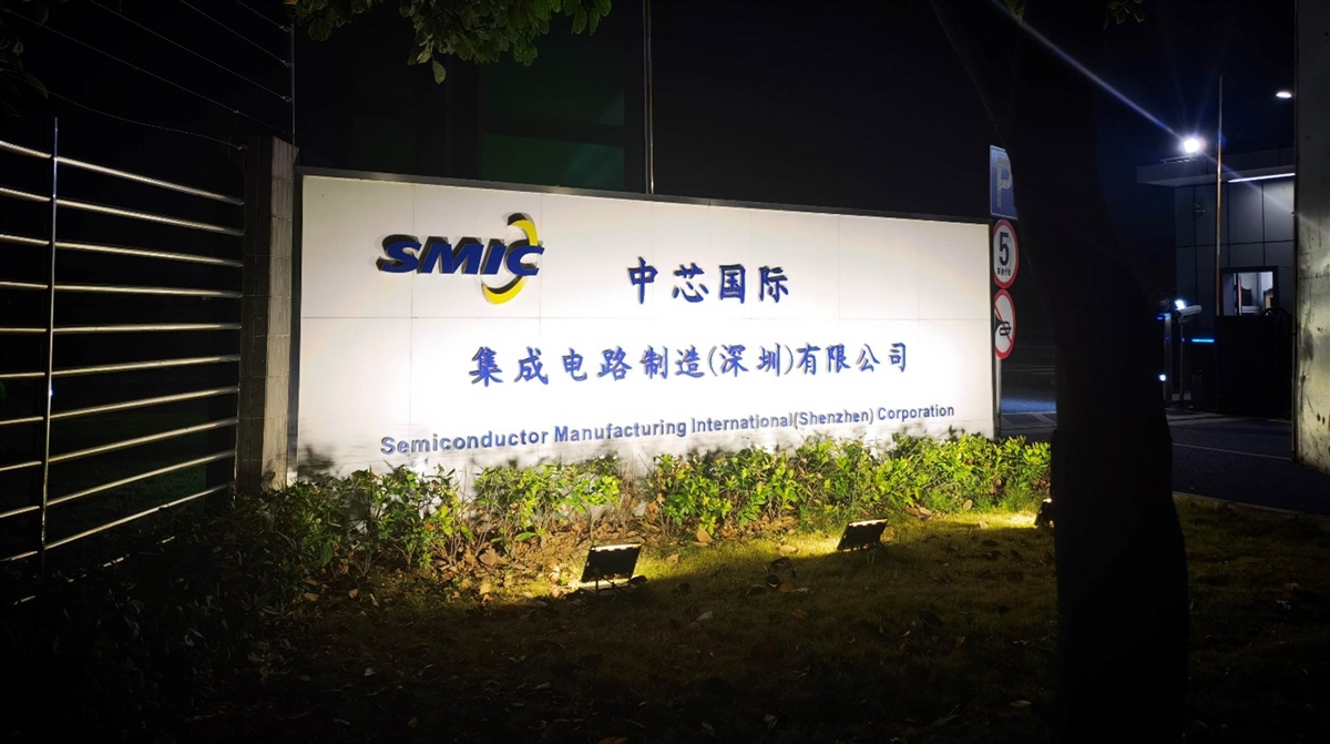
According to SMIC’s Q4 2022 financial statements, the company has invested about $197.5 million in R&D, accounting for the largest spending activity of the firm. The statement also shows a continued increase in expenses for R&D over $182.9 million in 3Q 2022 and $172 million in 4Q 2021.
At the organizational level, SMIC has aimed to “develop everything needed in house” from training local semiconductor engineers to collaborating with universities as well as hiring talent from Taiwan and the United States who helped train local talent.[167]
Apart from in-house training and R&D, SMIC’s innovation ecosystem has also been boosted by collaboration and partnerships with both industry and academia. Even as long as a decade ago, SMIC already had several R&D teams collaborating with partners from various organizations on new fabrication technologies dedicated to “mitigate risks as well as develop differentiated processes aimed at specific applications.” [168]
China’s Semiconductor Strategy
As early as 2014, Xi Jinping noted that “semiconductors [are] a core technology that China should produce domestically.” [169] Indeed, semiconductors represent a central part of Jinping’s “pledge to mobilize all means at [China’s] disposal to wrest technological supremacy from the United States and other nations.” [170]
The National IC Plan became the centerpiece of China’s semiconductor strategy in 2014, with China’s State Council setting a goal of China becoming a global leader in all segments of the semiconductor industry by 2030.171 The IC Plan called for at least $150 billion in government subsidies—from central, provincial, and municipal Chinese governments as well as a variety of state-owned enterprises (SOEs) from the technology sector and beyond—to enable China to become self-sufficient in every facet of the industry.172 The “Big Fund” was established to function as a national investment fund, offering targeted support for the development of the semiconductor industry.173 The 2014 fund raised 138.7 billion RMB ($23 billion) and the 2019 fund raised 200 billion RMB ($29 billion). In September 2023, Reuters reported that China was planning to start its most extensive state fund to date, with a target of 300 billion RMB ($41 billion). 174 America’s Department of Commerce estimates that China indeed reached its goal of pumping $150 billion into the sector over the past decade.175 Renowned semiconductor industry analyst Chris Miller suggested on a recent podcast that, if one adds up semiconductor-sector investments made by Chinese governments at all levels (national, provincial, city), China “has probably invested the equivalent of [America’s] CHIPS Act virtually every year since 2014.”176
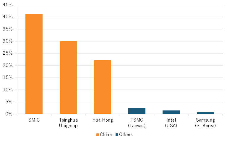
Massive industrial subsidization of Chinese semiconductor firms lies at the core of China’s project. As the Organization for Economic Cooperation and Development (OECD) has found, “Government support through below-market equity appears to be particularly large in the semiconductor industry and concentrated in one jurisdiction.” [177] The OECD’s study of 21 international semiconductor firms over the years 2014 to 2018 found that government support provided through “below-market equity” (i.e., effectively a subsidy) “amounted to $5-15 billion for just six semiconductor firms, four of which are from China” (these being Hua Hong, JCET, SMIC, and Tsinghua Unigroup). The report continued to note that, for SMIC and Tsinghua Unigroup, “total government support exceeded 30 percent of their annual consolidated revenue.” [178] In total, the OECD found that Chinese firms together received 86 percent of below-market equity injections identified in its study and concluded, “For the four Chinese firms covered by this study, government funds have committed equity funding of about $22 billion in total to date, with the largest share benefitting SMIC and Tsinghua Unigroup, and their subsidiaries. These four firms received about $10 billion of the initial $23 billion tranche of National IC Plan funding.” [179] With regard to SMIC, the OECD report found that state subsidies accounted for slightly over 40 percent of the company’s revenues from 2014 to 2018. [180] Of particular import, the OECD study found that there “notably appears to be a direct connection between equity injections by China’s government funds and the construction of new semiconductor fabs in the country.” [181]
When it comes to state subsidies at the firm level—that is, as a percentage of revenue for semiconductor manufacturers (from 2014 to 2018)—Chinese enterprises clearly led their foreign competitors by an order of magnitude. State subsidies accounted for slightly over 40 percent of SMIC’s revenues over this period: 30 percent for Tsinghua Unigroup, and 22 percent for Hua Hong. (See figure 18.) In contrast, this figure was minimal for TSMC, Intel, and Samsung, each, for which revenues identifiable as state subsidies accounted for, at most, 3 percent or less of their revenues over this period.
Figure 18: State subsidies as a percentage of revenue for chip fabs, 2014–2018[182]
Chinese semiconductor companies benefit from lower taxes, such as corporate income tax exemptions or reductions, tax credits for R&D, and tax or tariff reductions/exemptions for domestically produced or imported equipment and materials.[183] Subnational governments in China also sell land to Chinese semiconductor companies at reduced prices.[184]
As noted, in the seminal Made in China 2025 strategy, China set a goal of achieving 40 percent self-sufficiency in semiconductors by 2020 and 70 percent by 2025.[185] China’s “Information Innovation” project, locally called Xinchuang, aims to replace foreign with domestic suppliers of critical ICTs, including semiconductor technology.[186] As one report notes, China is seeking “to establish production processes largely free of Western equipment … This will be a multistage, multiyear process, starting with 40 nanometers and proceeding quickly, likely [in 2024], to 28 nanometers, and then 14, 12/10, and eventually 7 nanometers.”[187]
On April 12, 2024, The Wall Street Journal reported, “China’s push to replace foreign technology is now focused on cutting American chip makers out of the country’s telecommunications systems.” [188] The move would impact a variety of U.S. semiconductor companies, including AMD and Intel. The article notes that “[Chinese] officials earlier this year directed the nation’s largest telecom carriers to phase out foreign processors that are core to their networks by 2027.” [189] The effort is similar to one articulated in Document 79, which requires SOEs in finance, energy, and other sectors to replace foreign software in their IT systems by 2027. [190]
Elsewhere, the Chinese government has asked electric-vehicle makers, from BYD Co. to Geely Automobile Holdings Ltd., to sharply increase their purchases from local auto chipmakers as part of a campaign to reduce reliance on Western imports and boost China’s domestic semiconductor industry.191 China’s Ministry of Industry and Information Technology (MITI) is directly instructing Chinese automakers to avoid foreign semiconductors if at all possible.192 Such measures leave no doubt that import substitution and achieving self-sufficiency represents an essential goal of China’s semiconductor strategy.
Despite China’s massive investments in the sector, by early 2023, a sense had emerged in Beijing that they weren’t paying the expected dividends. Beijing felt that the “scientist-led approach has not delivered much progress,” nor has “the attempt to use market forces.” [193] Thus, in the wake of the March 2023 National People’s Congress, Beijing revamped oversight of its semiconductor industry by establishing a “leading small group” under vice premier Ding Xuexiang that will have oversight over all aspects of China’s new semiconductor strategy. [194] Triolo speculated that “a high-level decision may have been made that China needs a national-level SOE conglomerate to run overall semiconductor industry policy, in a manner similar to sectors like nuclear with CNNC and aerospace with CASIC,” though this has not yet come to pass. [195] Two aspects that do seem certain to change, however, are that China will increase its investments in basic R&D in semiconductor physics as well as critical technologies such as light sources for advanced lithography. That stems from a recognition that the Big Fund was “initially focused on manufacturing and design, and not enough attention paid to SME.” [196] Certainly, China is revamping its tactics to develop its semiconductor sector, but its hunger to dominate the sector remains unabated.
What Should America Do?
The United States made a major commitment to revitalizing the competitiveness of its semiconductor industry when Congress passed the 2022 CHIPS and Science Act. As of August 2024, the CHIPS program office has announced several notable investments from the fund, including $8.5 billion to support Intel’s construction of semiconductor facilities in four states, $6.6 billion to support three TSMC funds in Arizona, $6.5 billion for Samsung, and $1.5 billion to expand Global Foundries’ operations in New York, among others.197 Since 2020, semiconductor companies have committed over $300 billion to building and operating fabs in the United States.
On the research side, the CHIPS legislation features a massive $5 billion investment in America’s semiconductor industrial commons through the National Semiconductor Technology Consortium (NSTC), whose mission is “to ensure the U.S. leads the way in the next generation of semiconductor technologies by supporting the design, prototyping, and piloting of the latest semiconductor technologies; leveraging shared facilities and expertise to ensure innovators have access to critical capabilities; and building and sustaining a skilled and diverse semiconductor workforce.” [198] Further, the U.S. Department of Commerce has announced a $200 million investment in a CHIPS Manufacturing USA Institute to create a first-of-its-kind semiconductor manufacturing digital twin institute, which will allow innovators to replicate and experiment with physical manufacturing processes at low cost. [199] These represent critical initiatives whose success will depend on effective implementation and execution going forward. Also, with regard to America’s Manufacturing USA network—of which the CHIPS Institute will become the 18th institute—Congress should eliminate the automatic five- to seven-year federal funding sunset for the institutes and replace it with a five-year, metrics-based review program with minimum standards of performance focused on the advancement of technology and manufacturing readiness. [200]
The success of the multiple initiatives contemplated under the CHIPs and Science Act will depend on effective implementation and execution going forward.
The 25 percent ITC component of the CHIPS Act was one of its most powerful elements—companies could not be certain that they would win a loan or grant, but they were certain that they could take the 25 percent ITC if they put shovels in the ground. As such, Congress should extend the ITC through the end of this decade (it currently applies to planned construction beginning before January 1, 2027). Congress should also extend the 25 percent ITC to firms designing semiconductor chips, not just to those building semiconductor fabs.
The rapid expansion of China’s semiconductor industry—as has been the case for many other Chinese industries, from electric vehicles and solar panels to high-speed rail—has been powered in part through massive industrial subsidization of a nature and on a scale that clearly violates the country’s World Trade Organization (WTO) commitments. To address this, the United States should work with like-minded nations to update WTO rules to impose much stiffer conditions on, and penalties for, aggressive industrial subsidization. This should start with clarifying the definition of a “public body,” extending it to include state-influenced activities of entities such as state-owned enterprises or private firms. 202 Further reforms should insist on timely and complete notification of subsidies and establish a presumption of prejudice toward subsides not timely notified. 203 Rules should further obligate a subsidizing country to prove that a given subsidy does not inflict harm on others. On the basis of these investigations, OECD nations should consider import restrictions on massively subsidized Chinese chips.
The United States needs to dramatically expand and deepen its domestic STEM (science, technology, engineering, and mathematics) pipeline. For instance, SIA has found that America will face a shortage of 67,000 skilled workers in the semiconductor industry by 2030 (and a gap of 1.4 million such workers throughout the broader U.S. economy). [204] While it’s long been a strength for America’s innovation system that many of the world’s best and brightest students have been attracted to its universities, the dependence on foreign students at the upper echelons of America’s advanced degree programs creates a significant national security vulnerability. For instance, one 2017 study found that 81 percent of full-time graduate students in electrical engineering programs, and 79 percent in computer science, were international students. [205] Of those international students, a 2019 Congressional Research Service report found that nearly 70 percent of foreign students enrolled in STEM courses came from China and India. [206] To help build the domestic STEM talent pipeline, America should at least double its number of STEM high schools and establish an incentive program operated by the National Science Foundation to reward universities that do a better job of graduating B.S. STEM degrees. [207]
In its application of export controls on China, American administrations have to balance the competing interests of keeping advanced American technologies out of the national security apparatus of foreign competitors (and potentially of stymieing competitors’ industrial capabilities more broadly) against the reality that export controls reduce sales for American companies, which depend on those profits to reinvest in future generations of innovation—a reality particularly pertinent when U.S. semiconductor companies rely on the Chinese market for 36 percent of their sales. Export controls have become the go-to tool of choice for U.S. policy vis-à-vis China and has come at the expense of needed U.S. sales. As such, it’s imperative that U.S. semiconductor export controls vis-à-vis China be narrowly targeted—meaning strict controls on a few products in the “small garden, high wall” formulation—or focused on true “chokepoint technologies” such as SME. 208
Moreover, the United States should eschew the application of unilateral export controls and seek to develop a more ambitious and effective plurilateral approach to promulgate export controls among like-minded nations that have indigenous semiconductor production capacity, such as Germany, Japan, South Korea, Taiwan, the Netherlands, and the United Kingdom.[ 209] These nations should work together to establish a common understanding of both what threats are posed to the global semiconductor industry by enterprises from non-market economies not fundamentally competing on market-based terms as well as the pace and evolution of semiconductor technology.[ 210] Then, among themselves, these nations should establish working groups, outside the Wassenaar Arrangement (which was established in order to contribute to regional and international security and stability by promoting transparency and greater responsibility in transfers of conventional arms and dual-use goods and technologies), to develop descriptions of both the semiconductor technologies and related items that warrant controls (beyond what already exists) as well as establish common licensing policies.
To accomplish this would require allied nations such as Japan and South Korea to significantly modernize their export control regimes, laws, and policies as well. To assist other nations in modernizing their export control regimes, Congress should expand the remit and funding for the Export Control and Related Border Security (EXBS) Program at the U.S. Department of State. The EXBS program works with partner governments to identify regulatory and institutional gaps and provide technical and capacity-building assistance.[211] While the EXBS program has traditionally been more focused on export controls around weapons of mass destruction (WMDs) and national security-related technologies, its remit could be expanded to assist allied nations in further developing their capacity to evaluate export controls on advanced technologies.
As noted, China has been committed to the development of its semiconductor industry since at least the mid-2010s, well before the Trump and then Biden administrations began to impose export controls on this sector, so it is a canard that U.S. export controls have emboldened China to embark on a crash course to develop an indigenous semiconductor industry. That said, there is some evidence that U.S. export controls have since added urgency to Chinese efforts. In their paper, “Geopolitical Risk and Decoupling: Evidence from U.S. Export Controls” Crosignani et al. found that “by forbidding U.S. firms to export to a selected list of Chinese firms for national security reasons, export controls aim to generate a selective decoupling of U.S. firms from China.” [212] As they concluded:
{Export controls] prompt a supply chain reconfiguration away from Chinese customers, both those targeted by export controls and those that are not. This broad-based decoupling of U.S. firms from China is not offset by the creation of new supply chain relations in other countries. Indeed, the total number of customers declines, potentially inflicting collateral damage upon the same U.S. firms whose technology export controls are trying to protect.[213]
Crosignani et al.’s research shows the United States must tread very cautiously and purposefully to the extent it introduces semiconductor export controls on China.
Finally, the United States should continue to make strong use of the Entity Listing, particularly in instances where Chinese companies are found responsible for egregious cases of IP theft. China pilfers foreign technology by whatever means possible: The Chinese government has sponsored long-running state espionage programs targeting Western firms and research centers, and this technological espionage has carried over into cyberspace. Indeed, the acquisition of foreign semiconductor technology through IP theft has been a key pillar of Chinese strategy. For instance, in November 2018, the U.S. Department of Justice charged China’s Fujian Jinhua Integrated Circuit Co. with working to steal trade secrets from U.S. chipmaker Micron Technologies.[214] The incident spurred the Justice Department to launch a new initiative to combat foreign economic espionage and trade secret theft.
China’s policies to block U.S. tech companies from selling in China’s market are fundamentally antithetical to the commitments the country made in joining the WTO to conduct its economic and trade policies on a private enterprise-led, market-based, rules-governed trade in accordance with the foundational principles of national treatment, non-discrimination, and reciprocity.[215] To counter this, U.S. (and other allied nation) policymakers should develop new trade tools permitting the U.S. government to reciprocally exclude Chinese competitors from competing in U.S. markets in sectors where the Chinese are denying U.S. (and other foreign) firms market access. The European Union is already going down this path with China regarding its International Procurement Instrument (IPI), which will condition China’s access to European public procurement markets based on the extent to which China’s federal and provincial governments are permitting European firms to compete in its market.[216] Reciprocity should be a guiding principle of U.S. trade policy toward China.
Conclusion
The Chinese government fervently wishes to transform China into a leading competitor in the global semiconductor industry—in large part to reduce foreign dependency and increase domestic self-sufficiency in this strategically crucial industry—and has committed hundreds of billions of dollars to this cause. Should it achieve this, it will impose significant damage on foreign semiconductor firms because they will lose Chinese sales. Despite the gargantuan effort, it has thus far achieved only mixed returns. Despite pockets of advancement—notably in the design of AI chips and chips for mobile phones—overall, China likely remains about a half decade behind in its ability to design and manufacture at high volumes the most-advanced leading-edge semiconductor logic chips. As Hutcheson pointed out, “Ten years ago, [Chinese companies] were two generations behind. Five years ago, they were two generations behind, and now they’re still two generations behind.” China likely trails even more significantly in SME. To be sure, Huawei’s effort to apply double patterning (the SASQ example) shows that Chinese semiconductor developers are attempting to be as innovative as they can possibly be in process innovation, at least with the assets and technologies available, even if these are clearly behind the global frontier currently. Ultimately, Chinese enterprises are innovating as rapidly as they’re able to in this industry—and they have achieved some notable achievements and advancements—but overall, they remain behind global leaders in the semiconductor industry. But if allied nations rest on their laurels, they risk seeing a significant diminution of their industries.
Acknowledgment
ITIF wishes to thank the Smith Richardson Foundation for supporting research on the question, “Can China Innovate?” Other reports in this series will cover artificial intelligence, biopharmaceuticals, chemicals, electric vehicles and batteries, nuclear power, quantum computing, and robotics. The author would also like to thank Ian Tufts and Robert Atkisnon for their assistance with this report. (Search #ChinaInnovationSeries on itif.org.)
Any errors or omissions are the author’s responsibility alone.
About the Author
Stephen Ezell is vice president for global innovation policy at the Information Technology and Innovation Foundation (ITIF) and director of ITIF’s Center for Life Sciences Innovation. He also leads the Global Trade and Innovation Policy Alliance. His areas of expertise include science and technology policy, international competitiveness, trade, and manufacturing.
About ITIF
The Information Technology and Innovation Foundation (ITIF) is an independent 501(c)(3) nonprofit, nonpartisan research and educational institute that has been recognized repeatedly as the world’s leading think tank for science and technology policy. Its mission is to formulate, evaluate, and promote policy solutions that accelerate innovation and boost productivity to spur growth, opportunity, and progress. For more information, visit itif.org/about.
Endnotes
[1]. Stephen Ezell, “An Allied Approach to Semiconductor Leadership” (ITIF, September 2020), https://itif.org/publications/2020/09/17/allied-approach-semiconductor-leadership/.
[2]. Hanna Dohmen et al., “The Limits of the China Chip Ban,” Foreign Affairs, July 24, 2024, https://www.foreignaffairs.com/china/limits-china-chip-ban.
[3]. Michael Schuman, “China Is Losing the Chip War,” The Atlantic, June 6, 2024, https://www.theatlantic.com/international/archive/2024/06/china-microchip-technology-competition/678612/.
[4]. Anton Shilov, “Chinese Chip Sector Is Five Generations Behind the World: The Gap Will Expand,” Tom’s Hardware, August 15, 2023, https://www.tomshardware.com/news/chinese-chip-sector-is-five-generations-behind-the-world-the-gap-will-expand.
[5]. Schuman, “China Is Losing the Chip War.”
[7]. SIA, “Global Semiconductor Sales Decrease 8.2% in 2023; Market Rebounds Late in Year,” news release, February 5, 2024, https://www.semiconductors.org/global-semiconductor-sales-decrease-8-2-in-2023-market-rebounds-late-in-year/; Ondrej Burkacky, Julia Dragon, and Nikolaus Lehmann, “The semiconductor decade: A trillion-dollar industry” (McKinsey Global Institute (MGI), April 2022), https://www.mckinsey.com/industries/semiconductors/our-insights/the-semiconductor-decade-a-trillion-dollar-industry#/.
[10]. ASML, "The road to EUV," https://www.asml.com/en/products/euv-lithography-systems.
[11]. Richard Windsor, “China vs. USA – 7nm debate,” Radio Free Mobile, September 7, 2023, https://www.radiofreemobile.com/china-vs-usa-7nm-debate/.
[12]. Arjun Kharpal, “Netherlands, home to a critical chip firm, follows U.S. with export curbs on semiconductor tools,” CNBC, June 30, 2023, https://www.cnbc.com/2023/06/30/netherlands-follows-us-with-semiconductor-export-restrictions-.html.
[13]. Burkacky, Dragon, and Lehmann, “The semiconductor decade: A trillion-dollar industry.”
[14]. Ezell, “An Allied Approach to Semiconductor Leadership,” 15.
[15]. Sandra Barbosu, “Not Again: Why the United States Can’t Afford to Lose Its Biopharma Industry” (ITIF, February 2024), https://itif.org/publications/2024/02/29/not-again-why-united-states-cant-afford-to-lose-biopharma-industry/.
[16]. "China is quietly reducing its reliance on foreign chip technology," The Economist, February 13, 2024, https://www.economist.com/business/2024/02/13/china-is-quietly-reducing-its-reliance-on-foreign-chip-technology.
[17]. Ezell, “An Allied Approach to Semiconductor Leadership.”
[18]. Jamie Gaida et al., “ASPI’s Critical Technology Tracker: The global race for future power” (Australian Strategic Policy Institute (ASPI), Policy Brief Report No. 69, 2023), 22, https://www.aspi.org.au/report/critical-technology-tracker.
[21]. Stephen Ezell, “The CHIPS Program Office Needs to Think Like Economic Developers, Not Bankers,” Innovation Files, February 1, 2024, https://itif.org/publications/2024/02/01/the-chips-program-office-needs-to-think-like-economic-developers-not-bankers/.
[22]. Jordan Bish et al., “A new dawn for European chips” (Deloitte, November 2022), https://www2.deloitte.com/xe/en/insights/industry/technology/semiconductor-chip-shortage-supply-chain.html.
[23]. “Who’s Winning the US-China Chip War?” CITI Global Insights, October 11, 2023, https://www.citigroup.com/global/insights/global-insights/who-s-winning-the-us-china-chip-war-.
[24]. “Intel CEO Claims China’s Chip Manufacturing Lags Behind by 10 Years, Gap to Persist,” TrendForce, January 19, 2024, https://www.trendforce.com/news/2024/01/19/intel-ceo-claims-chinas-chip-manufacturing-lags-behind-by-10-years-gap-to-persist.
[25]. Daniel Araya, “Will China Dominate the Global Semiconductor Market?” (Centre for International Governance Innovation, January 2024), https://www.cigionline.org/articles/will-china-dominate-the-global-semiconductor-market/.
[26]. Dieter Ernst, “From Catching Up to Forging Ahead: China’s Policies for Semiconductors” (East-West Center Special Study, 2015), https://papers.ssrn.com/sol3/papers.cfm?abstract_id=2744974.
[27]. Stephen Ezell, “Moore’s Law Under Attack: The Impact of China’s Policies on Global Semiconductor Innovation” (ITIF, February 2021), https://itif.org/publications/2021/02/18/moores-law-under-attack-impact-chinas-policies-global-semiconductor/.
[28]. Andrew David et al., “Foundational Fabs: China’s Use of Non-Market Policies to Expand Its Role in the Semiconductor Supply Chain” (Silverado Policy Accelerators, October 2023), 15, https://silverado.org/news/report-foundational-fabs-chinas-use-of-non-market-policies/.
[29]. Schuman, “China Is Losing the Chip War.”
[31]. Comments of Jimmy Goodrich at roundtable discussion on “Is China’s Semiconductor Industry Innovative?” October 25, 2023.
[32]. National Science Foundation, “Science & Engineering Indicators 2018” (Appendix Table 6-14), accessed July 14, 2020, https://nsf.gov/statistics/2018/nsb20181/assets/1235/tables/at06-14.pdf.
[33]. SIA, "2024 Factbook" (SIA, 2024), 6, https://www.semiconductors.org/wp-content/uploads/2024/05/SIA-2024-Factbook.pdf.
[38]. Synopsys, “What is EDA (Electronic Design Automation)?” https://www.synopsys.com/glossary/what-is-electronic-design-automation.html.
[39]. Michael Laha, “PRC Pursues Chip Design Software Dominance,” China Brief, March 15, 2024, https://jamestown.org/program/prc-pursues-eda-software-dominance/.
[41]. “China is quietly reducing its reliance on foreign chip technology,” The Economist.
[42]. Laha, "PRC Pursues Chip Design Software Dominance."
[43]. Misha Lu, “Chinese EDA Champion Empyrean Can Now ‘Fully Support’ 7nm; Sees 1Q23 Sales Growth,” DigiTimes, May 22, 2023, https://www.digitimes.com/news/a20230522VL203/7nm-china-eda-ic-design-distribution.html.
[44]. “Nanjing hosts China’s first national EDA innovation center,” Jiangsu Now, June 30, 2023, https://english.jschina.com.cn/23264/202306/t20230630_7994398.shtml.
[45]. Laha, "PRC Pursues Chip Design Software Dominance."
[46]. China National EDA Innovation Center, “Document from the Organizing Committee of the Integrated Circuit EDA Elite Challenge,” https://edaicisc.oss-cn-shanghai.aliyuncs.com/file/cacheFile/2023/10/19/ceb2d08f6ef14184be0b0b2de3796eb8.pdf.
[48]. Laha, "PRC Pursues Chip Design Software Dominance."
[50]. David et al., “Foundational Fabs,” 16.
[51]. “China chip design expert warns of losses due to industry overcrowding, says more cautious path to self-sufficiency is needed,” South China Morning Post, November 12, 2023, https://finance.yahoo.com/news/china-chip-design-expert-warns-093000095.html.
[52]. David et al., “Foundational Fabs,” 16.
[54]. Synopsys, “RISC-V Definition,” https://www.synopsys.com/glossary/what-is-risc-v.html.
[55]. Don Clark and Ana Swanson, “The Next Frontier in the U.S.-China Battle Over Chips,” The New York Times, January 10, 2024, https://www.nytimes.com/2024/01/10/technology/risc-v-china-united-states-chips-security.html.
[56]. Kezia Leung, "RISC-V Expanding In China," RISC-V, August 14, 2023, https://riscv.org/blog/2023/08/risc-v-expanding-in-china/.
[57]. Paul Triolo, “A New Era for the Chinese Semiconductor Industry: Beijing Responds to Export Controls” American Affairs Vol. VIII, No. 1 (Spring 2024): 38, https://americanaffairsjournal.org/2024/02/a-new-era-for-the-chinese-semiconductor-industry-beijing-responds-to-export-controls/.
[58]. Clark and Swanson, “The Next Frontier in the U.S.-China Battle Over Chips.”
[59]. Nigel Cory, “The US-China Tech Conflict Fractures Global Technical Standards: The Case of Semiconductors and the RISC-V Standard,” Innovation Files, July 19, 2024, https://itif.org/publications/2024/07/19/the-us-china-tech-conflict-fractures-global-technical-standards/.
[60]. Clark and Swanson, “The Next Frontier in the U.S.-China Battle Over Chips.”
[62]. “China is quietly reducing its reliance on foreign chip technology,” The Economist.
[63]. Schuman, “China Is Losing the Chip War.”
[64]. Tracy Alloway and Joe Weisenthal, “China Made a Chip Breakthrough That Shocked The World,” Bloomberg, December 7, 2023, https://www.bloomberg.com/news/articles/2023-12-07/huawei-mate-60-pro-chip-breakthrough-shocks-computing-world.
[65]. Dylan Patel and Doug O’Loughlin commenting on Oddlots podcast, December 7, 2023; Alloway and Weisenthal, “China Made a Chip Breakthrough That Shocked The World.”
[66]. Patel and O’Loughlin on Oddlots podcast.
[68]. Dylan Patel, “China AI & Semiconductors Rise: US Sanctions Have Failed,” SemiAnalysis, September 12, 2023, https://www.semianalysis.com/p/china-ai-and-semiconductors-rise.
[69]. Semiconductor Engineering, “Double Patterning,” https://semiengineering.com/knowledge_centers/manufacturing/patterning/double-patterning; Windsor, “China vs. USA – 7nm debate.”
[71]. Patel, “China AI & Semiconductors Rise: US Sanctions Have Failed.”
[72]. Yuan Gao and Debby Wu, “Huawei Tests Brute-Force Method for Making More Advanced Chips,” Bloomberg, March 22, 2024, https://www.bloomberg.com/news/articles/2024-03-22/huawei-tests-brute-force-method-for-making-more-advanced-chips.
[73]. Anton Shilov, “SMIC and Huawei could use quadruple patterning for China-made 5nm chips: Report,” Tom’s Hardware, March 24, 2024, https://www.tomshardware.com/tech-industry/semiconductors/smic-and-huawei-could-use-quadruple-patterning-for-chinese-5nm-chips-report.
[75]. Patel, “China AI & Semiconductors Rise: US Sanctions Have Failed.”
[78]. Hassan Mujtaba, “Birentech Details China’s Most Powerful GPU, The Biren BR100: 1074mm2 on 7nm, 77 Billion Transistors, Up To 2.8x Faster Than NVIDIA Ampere at 550W,” WCCF Tech Inc., August 22, 2022, https://wccftech.com/birentech-china-most-powerful-gpu-biren-br100-architecture-disclosed-2-8x-faster-than-nvidia-ampere/.
[80]. Luciano Ballerano, “How NVIDIA’s CUDA Ecosystem Powers Innovation,” March 30, 2024, https://www.linkedin.com/pulse/how-nvidias-cuda-ecosystem-powers-innovation-luciano-ballerano-cmcwf/.
[81]. Zo Ahmed, “China’s Loongson claims its latest CPUs are a match for Intel’s 10th-gen in single-core performance,” Techspot, April 28, 2024, https://www.techspot.com/news/102771-chinese-chipmaker-loongson-new-3b6600-3b7000-chips-narrow.html.
[83]. Fanny Potkin and Eduardo Baptista, “Chinese firms make headway in producing high bandwidth memory for AI chipsets,” Reuters, May 15, 2024, https://www.reuters.com/technology/chinese-firms-make-headway-producing-high-bandwidth-memory-ai-chipsets-2024-05-14/.
[84]. China Tech Threat (CTT), “Every Chip Matters” (CTT, April 2023), 5, https://chinatechthreat.com/wp-content/uploads/2023/05/CTT-EveryChipMatters-Final-Paper.pdf.
[85]. Sujai Shivakumar, Charles Wessner, and Thomas Howell, “The Strategic Importance of Legacy Chips” (CSIS, March 2023), https://www.csis.org/analysis/strategic-importance-legacy-chips.
[86]. “Intel pours €30bn into chip manufacturing in Europe,” Financial Times, March 15, 2022, https://www.ft.com/content/3f7e4a87-f0c4-469a-b0cf-7bb3570e31f4.
[87]. Zeyi Yang, “Chinese chips will keep powering your everyday life: The war over advanced semiconductors,” MIT Technology Review, January 4, 2023, https://www.technologyreview.com/2023/01/04/1066136/chinese-legacy-chips-advantage/.
[88]. Megha Mandavia, “How China Could Swamp India’s Chip Ambitions,” The Wall Street Journal, March 16, 2024, https://www.wsj.com/tech/how-china-could-swamp-indias-chip-ambitions-b01c4fcc.
[89]. Coco Feng, “China’s semiconductor output jumps 40% in first quarter amid growing dominance in legacy chips,” South China Morning Post, April 16, 2024, https://www.scmp.com/tech/tech-war/article/3259221/chinas-semiconductor-output-jumps-40-first-quarter-amid-growing-dominance-legacy-chips.
[90]. Andrew David et al., “Foundational Fabs,” 19.
[93]. Simone Bertolazzi, “Semiconductor memory: China’s ambition shows no signs of slowing down,” Yole Group, May 10, 2023, https://www.yolegroup.com/strategy-insights/semiconductor-memory-chinas-ambition-shows-no-signs-of-slowing-down/.
[94]. SOS International, “Blue Heron: Yangtze Memory Technologies Co. (YMTC)” (SOS International, December 2020), 6.
[95]. He Shujing and Mo Yelin, “China creates new memory chip champ, but will customers come?” Nikkei Asia, August 18, 2020, https://asia.nikkei.com/Spotlight/Caixin/China-creates-new-memory-chip-champ-but-will-customers-come.
[96]. Triolo, “A New Era for the Chinese Semiconductor Industry,” 34.
[98]. Che Pan, "China’s top memory chip maker YMTC takes latest step to become a global market leader, but US sanctions could derail its ambitions," South China Morning Post, December 1, 2022, https://www.scmp.com/tech/tech-war/article/3201715/chinas-top-memory-chip-maker-ymtc-takes-latest-step-become-global-market-leader-us-sanctions-could.
[99]. Jiaxing Li, “Tech war: China’s top memory chip maker YMTC faces headwinds amid reports US is weighing equipment export ban,” South China Morning Post, August 3, 2022, https://www.scmp.com/tech/tech-war/article/3187606/tech-war-chinas-top-memory-chip-maker-ymtc-faces-headwinds-amid.
[100]. “Apple reportedly paused plans to buy memory chips from China’s YMTC,” HardwareZone.com, October 18, 2022, https://www.hardwarezone.com.sg/tech-news-apple-reportedly-paused-plans-buy-memory-chips-chinas-ymtc.
[101]. Ann Cao and Che Pan, “Top Chinese memory chip maker YMTC said to be laying off 10 per cent of workforce after US sanctions,” South China Morning Post, January 30, 2023, https://www.scmp.com/tech/big-tech/article/3208490/top-chinese-memory-chip-maker-ymtc-said-be-laying-10-cent-workforce-after-us-sanctions.
102. Bertolazzi, “Semiconductor memory.”
[103]. Cheng Ting-Fang, “China’s CXMT aims to build country’s first advanced memory chips for AI,” Nikkei Asia, February 1, 2024, https://asia.nikkei.com/Business/Tech/Semiconductors/China-s-CXMT-aims-to-build-country-s-first-advanced-memory-chips-for-AI.
[105]. Triolo, “A New Era for the Chinese Semiconductor Industry,” 34.
[106]. David et al., “Foundational Fabs,” 20.
[107]. Potkin and Baptista, “Chinese firms make headway in producing high bandwidth memory for AI chipsets.”
[108]. ASML, “6 crucial steps in semiconductor manufacturing,” https://www.asml.com/en/news/stories/2021/semiconductor-manufacturing-process-steps.
[109]. Triolo, “A New Era for the Chinese Semiconductor Industry,” 44.
[113]. In February 2024, Intel CEO Gelsinger noted, “Today we are announcing Intel 14A for the first time. You can think about this for 1.4 nanometer technology.” Yifan Yu, “Intel joins 1.4-nanometer chip race against TSMC and Samsung,” Nikkei Asia, February 22, 2024, https://asia.nikkei.com/Business/Tech/Semiconductors/Intel-joins-1.4-nanometer-chip-race-against-TSMC-and-Samsung; Anton Shilov, “TSMC mentions 1.4nm process tech for the first time, says 2nm remains on track,” Tom’s Hardware, December 13, 2023, https://www.tomshardware.com/tech-industry/manufacturing/tsmc-mentions-14nm-process-tech-for-the-first-time-says-2nm-remains-on-track.
[114]. Anton Shilov, “Chinese company claims chipmaking tool breakthrough — announces 28nm-capable litho tool,” Tom’s Hardware, December 20, 2023, https://www.tomshardware.com/tech-industry/chinese-company-claims-chip-making-tool-breakthrough-announces-28nm-capable-litho-tool.
[115]. “China is quietly reducing its reliance on foreign chip technology,” The Economist. Source: Bernstein Research.
[116]. Congressional Research Service, “Semiconductors and the Semiconductor Industry” (CRS, April 2023), 20, https://sgp.fas.org/crs/misc/R47508.pdf.
[117]. Saif M. Khan, Alexander Mann, and Dhalia Peterson, “The Semiconductor Supply Chain: Assessing National Competitiveness” (Center for Security and Emerging Technology (CSET), January 2021), 8, https://cset.georgetown.edu/wp-content/uploads/The-Semiconductor-Supply-Chain-Issue-Brief.pdf.
[118]. Akhil Thadani and Gregory C. Allen, “Mapping the Semiconductor Supply Chain” (Center for Strategic and International Studies, May 2023), 11, https://www.csis.org/analysis/mapping-semiconductor-supply-chain-critical-role-indo-pacific-region.
[119]. Chris Miller and David Talbot, “Mexico’s Microchip Advantage,” Foreign Affairs, August 28, 2023, https://www.foreignaffairs.com/mexico/mexicos-microchip-advantage-semiconductor-china; Stephen Ezell, “Assessing the Dominican Republic’s Readiness to Play a Greater Role in Global Semiconductor and PCB Value Chains” (ITIF, January 2024), https://itif.org/publications/2024/01/29/dr-semiconductor-readiness/.
[120]. Saif M. Khan and Alexander Mann, “AI Chips: What They Are and Why They Matter” (CSET, April 2020), https://cset.georgetown.edu/publication/ai-chips-what-they-are-and-why-they-matter/.
[121]. Jane Lanhee Lee, “A New Front Is Opening Up in the US-China Conflict Over Chips,” Bloomberg, November 20, 2023, https://www.bloomberg.com/news/features/2023-11-21/tech-war-us-china-competition-moves-into-advanced-chip-packaging.
[123]. Triolo, “A New Era for the Chinese Semiconductor Industry.”
[125]. Comments of Jimmy Goodrich at roundtable discussion on “Is China’s Semiconductor Industry Innovative?” October 25, 2023.
[126]. Ben Hernandez, “Breakthrough in China Should Spur Innovation in Semiconductors,” VettaFi, August 30, 2023, https://www.etftrends.com/leveraged-inverse-channel/breakthrough-china-spur-novation-in-semiconductors/.
[127]. Leng Shumei, “Chinese, US researchers jointly develop new type of stable semiconductor graphene with 10 times higher performance than silicon,” Global Times, January 15, 2024, https://www.globaltimes.cn/page/202401/1305386.shtml.
[128]. Zhang Tong, “Chinese scientists create world’s most energy-efficient AI chips for mobile devices,” March 23, 2024, South China Morning Post, https://www.scmp.com/news/china/science/article/3256211/chinese-scientists-create-worlds-most-energy-efficient-ai-chips-mobile-devices.
[131]. Stephen Chen, “China’s new ultra-fast chip could double the pace of electronic warfare: research team,” South China Morning Post, July 30, 2024, https://www.scmp.com/news/china/science/article/3272480/chinas-new-ultra-fast-chip-could-double-pace-electronic-warfare-research-team.
[132]. SIA, “2023 Factbook,” 3.
[133]. Ezell, “Moore’s Law Under Attack.”
[134]. SIA, “2023 Factbook,” 3.
[135]. European Commission (EC), “The 2023 EU Industrial R&D Investment Scoreboard” (EC, 2023), https://publications.jrc.ec.europa.eu/repository/handle/JRC135576.
[136]. Gaida et al., “ASPI’s Critical Technology Tracker: The global race for future power,” 22.
[139]. Edd Cavanna, “Semiconductor patents rise by 59% in five years to reach to record high,” news release, Mathys & Squire, https://www.mathys-squire.com/insights-and-events/news/semiconductor-patents-rise-by-59-in-five-years-to-reach-to-record-high/.
[140]. World Intellectual Property Organization (WIPO), “WIPO statistics database (4 – Patent publications by technology, Total count by filing office, 8 – Semiconductors; 1980, 2022,” accessed March 27, 2024), https://www3.wipo.int/ipstats/ips-search/patent.
[141]. WIPO, “Patent Cooperation Treaty (PCT),” https://www.wipo.int/treaties/en/registration/pct/.
[143]. OECD.Stat, “IP5 Patent Families,” accessed April 16, 2024.
[144]. OECD Statistics, Patents by technology (Patents by IPC – Section G; G21B, G21C, G21D, G21F, G21G, G21H, G21J, G21K; 1999, 2020; accessed April 16, 2024), https://stats.oecd.org/.
[145]. National Science Board, “Science and Engineering Indicators 2024 Table SINV-10: USPTO utility patents granted in semiconductors, by selected region, country, or economy: 1998–2022,” accessed March 21, 2024, https://ncses.nsf.gov/pubs/nsb20241/data/table/SINV-10.
[146]. Olivia Rafferty, “China’s surge in semiconductor innovation,” IAM, September 19, 2023 (citing data from LexisNexis), https://www.iam-media.com/article/chinas-surge-in-semiconductor-innovation.
[154]. Oliver Peckham, “Chinese Startup Biren Details BR100 GPU,” HPCWire, August 20, 2022, https://www.hpcwire.com/2022/08/22/chinese-startup-biren-details-br100-gpu/.
[160]. Triolo, “A New Era for the Chinese Semiconductor Industry.”
[161]. Arran Hope, “China’s top 10 semiconductor firms,” The China Project, February 3, 2023, https://thechinaproject.com/2023/02/03/chinas-top-10-semiconductor-firms/.
[162]. Jason Abt, “SMIC’s Next Generation Process,” TechInsights, https://www.techinsights.com/blog/smics-next-generation-process.
[163]. TechInsights, “SMIC 7nm is truly 7nm technology, how it compares to TSMC 7nm,” https://www.techinsights.com/blog/smic-7nm-truly-7nm-technology-how-it-compares-tsmc-7nm.
[165]. Deena Theresa, “China’s top chipmaker SMIC just achieved an Intel-like breakthrough,” Interesting Engineering, August 30, 2022, https://interestingengineering.com/innovation/chinas-top-chipmaker-smic-7-nm-breakthrough.
[166]. TechInsights, “Comparing SMIC 7nm vs TSMC 7nm.”
[169]. “Silicon Supremacy,” Financial Times (podcast), https://www.ft.com/content/7bf0f79b-dea7-49fa-8253-f678d5acd64a.
[170]. Mackenzie Hawkins, “China Urges EV Makers to Buy Local Chips as US Clash Deepens,” Bloomberg, March 15, 2024, https://www.bloomberg.com/news/articles/2024-03-15/china-urges-byd-ev-makers-to-buy-chinese-chips-as-tensions-with-us-escalate.
[171]. James A. Lewis, “Learning the Superior Techniques of the Barbarians” (Center for Strategic and International Studies, January 2019), 2, https://csis-website-prod.s3.amazonaws.com/s3fs-public/publication/190115_Lewis_Semiconductor_v6.pdf.
[172]. Robert D. Atkinson, Nigel Cory, and Stephen Ezell, “Stopping China’s Mercantilism: A Doctrine of Constructive, Alliance-Backed Confrontation” (ITIF, March 2017), 15, https://itif.org/publications/2017/03/16/stopping-chinas-mercantilism-doctrine-constructive-alliance-backed.
[173]. Andrew David et al., “Foundational Fabs,” 15.
[174]. Julie Zhu, “Exclusive: China to launch $40 billion state fund to boost chip industry,” Reuters, September 5, 2023, https://www.reuters.com/technology/china-launch-new-40-bln-state-fund-boost-chip-industry-sources-say-2023-09-05/.
[175]. “China is quietly reducing its reliance on foreign chip technology,” The Economist.
[176]. “Silicon Supremacy,” Financial Times.
[177]. Organization for Economic Cooperation and Development (OECD), “Measuring distortions in international markets: The semiconductor value chain” (OECD, November 2019), 8, https://www.oecd-ilibrary.org/docserver/8fe4491d-en.pdf.
[180]. Dan Wang, “A Bumpier Road to Semiconductor Supremacy,” Gravel Dragonomics, July 14, 2020.
[181]. OECD, “Measuring distortions in international markets: The semiconductor value chain,” 9.
[183]. David et al., “Foundational Fabs,” 14.
[186]. “China is quietly reducing its reliance on foreign chip technology,” The Economist.
[187]. Triolo, “A New Era for the Chinese Semiconductor Industry.”
[188]. Liza Lin, “China Tells Telecom Carriers to Phase Out Foreign Chips in Blow to Intel, AMD,” The Wall Street Journal, April 12, 2024, https://www.wsj.com/tech/china-telecom-intel-amd-chips-99ae99a9.
[190]. Liza Lin, “China Intensifies Push to “Delete America” From Its Technology,” The Wall Street Journal, March 7, 2024, https://www.wsj.com/world/china/china-technology-software-delete-america-2b8ea89f.
[191]. Hawkins, “China Urges EV Makers to Buy Local Chips as US Clash Deepens.”
[193]. Triolo, “A New Era for the Chinese Semiconductor Industry,” 36-37.
[197]. NIST, “Chips for America,” https://www.nist.gov/chips; Asa Fitch and Annie Linskey, “Intel Gets $8.5 Billion Award For U.S. Chip-Plant Construction,” The Wall Street Journal, March 20, 2024, https://www.wsj.com/tech/intel-gets-8-5-billion-award-for-u-s-chip-plant-construction-4b3c42ec; Asa Fitch, “Billions Start Flowing to Chip Makers for New U.S. Factories,” The Wall Street Journal, February 19, 2024, https://www.wsj.com/tech/billions-start-flowing-to-chip-makers-for-new-u-s-factories-4d832ffd.
[198]. The White House, “FACT SHEET: Biden-Harris Administration Announces Over $5 Billion from the CHIPS and Science Act for Research, Development, and Workforce,” news release, February 9, 2024, https://www.whitehouse.gov/briefing-room/statements-releases/2024/02/09/fact-sheet-biden-harris-administration-announces-over-5-billion-from-the-chips-and-science-act-for-research-development-and-workforce/.
200. Stephen Ezell, “Policy Recommendations to Stimulate U.S. Manufacturing Innovation” (ITIF, May 2020), https://itif.org/publications/2020/05/18/policy-recommendations-stimulate-us-manufacturing-innovation/.
[202]. Office of the United States Trade Representative, “Joint Statement on Trilateral Meeting of the Trade Ministers of the United States, Japan, and the European Union,” news release, May 31, 2018, https://ustr.gov/about-us/policy-offices/press-office/press-releases/2018/may/joint-statement-trilateral-meeting.
[203]. Stephen Ezell, “Strengthening Subsidies Rules to Tackle Trade-Distortions: Perspectives From the High-Tech Sector” (power point presentation at 2019 WTO Public Forum, “Trading Forward: Adapting to a Changing World,” October 11, 2019).
[204]. Semiconductor Industry Association, “America Faces Significant Shortage of Tech Workers in Semiconductor Industry and Throughout U.S. Economy,” news release, July 25, 2023, https://www.semiconductors.org/america-faces-significant-shortage-of-tech-workers-in-semiconductor-industry-and-throughout-u-s-economy/.
[207]. Stephen Ezell, “Assessing the State of Digital Skills in the U.S. Economy” (ITIF, November 2021), https://itif.org/publications/2021/11/29/assessing-state-digital-skills-us-economy/.
[208]. Robert D. Atkinson, “Stronger Semiconductor Export Controls on China Will Likely Harm Allied Semiconductor Competitiveness,” Innovation Files, October 12, 2023, https://itif.org/publications/2023/10/12/stronger-semiconductor-export-controls-on-china-will-likely-harm-allied-semiconductor-competitiveness/.
[209]. Proposal suggested by Kevin Wolf in phone call with Stephen Ezell, July 13, 2020.
[210]. Ezell, “An Allied Approach to Semiconductor Leadership.”
[211]. U.S. Department of State, “The EXBS Program,” https://www.state.gov/export-control-and-related-border-security-program/.
[212]. Matteo Crosignani, “Geopolitical Risk and Decoupling: Evidence from U.S. Export Controls” Federal Reserve Bank of New York, No. 1096 (April 2024), https://www.newyorkfed.org/research/staff_reports/sr1096.
[215]. Stephen Ezell, “False Promises II: The Continuing Gap Between China’s WTO Commitments and Its Practices” (ITIF, July 2021), https://itif.org/publications/2021/07/26/false-promises-ii-continuing-gap-between-chinas-wto-commitments-and-its/.
[216]. James Killick and Jia Liu, “A new European trade tool: The first investigation under the International Procurement Instrument,” White & Case, April 29, 2024, https://www.whitecase.com/insight-alert/new-european-trade-tool-first-investigation-under-international-procurement.